

 Manufacturers
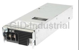
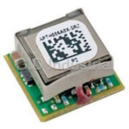
GE CRITICAL POWER CAR0812DCXXXZ01A
Description
850 W, - 36 -- 75 VDC Vin, Single Output, 12 VDC@70.8 A DC-DC Converter
Part Number
CAR0812DCXXXZ01A
Price
Request Quote
Manufacturer
GE CRITICAL POWER
Lead Time
Request Quote
Category
Capacitors » DC-DC Converter
Specifications
Manufacturer
GE Critical Power
Manufacturers Part #
CAR0812DCXXXZ01A
Industry Aliases
CAR0812DCXXXZ01A
Brand
GE Critical Power
Series
CAR0812DC
Factory Pack Quantity
5
Cooling Method
Air-Cooled
Dimensions
9.54 x 3.38 x 1.61"
Efficiency
92%
Input Type
DC
Input Voltage Nominal
- 48 VDC / - 60 VDC
Isolation
1500 VDC
Mechanical Style
Isolated
Mounting
Rack Mount
Number of Outputs
1
Operating Temperature
- 10 to + 70°C
Output Amps 1
70.8 A
Output Voltage V1 Nominal
12 VDC
Package Type
Enclosed
Power
850 W
Subcategory
DC-DC Converter
Datasheet

Extracted Text
Data Sheet GE CAR0812DC Series DC-DC Converter Input: -36V to -75V ; Output: +12 V @ 850W; 3.3V or 5 V @ 1A DC DC DC DC DC Features RoHS Compliant Reverse input voltage protection 2 front panel LEDs: LED 1-input, LED2-[output, fault, over temp] Remote ON/OFF control of the 12V output DC 12Vdc Regulation: set point ±0.2%, overall ±3% 12Vdc programmable between 10.8 – 13.2VDC Active load sharing on the 12V output Firmware adjustable overload set point of 12V output Standby orderable either as 3.3VDC or 5VDC Efficiency: typically 92% @ 50% load Exceeds 80plus GOLD standard Auto recoverable protection Applications Hot insertion/removal (hot plug) • 12V distributed power architectures DC Operating temperature: -10 - 70C, 2 + Digital status & control: I C and PMBus serial bus • Mid-End Servers nd * † ‡ EN/IEC/UL60950-1 2 edition; UL , CSA and VDE • Blade Servers § CE mark meets 2006/95/EC directive • Storage Area Networks EMI: class B FCC docket 20780 part 15, EN55022 • Routers/Switches Meets EN6100 immunity and transient standards • Enterprise Networks • Advanced workstations Description The CAR0812DC series of converters provide highly efficient isolated power from 48/60Vdc -input systems. Offered in the industry standard compact 1U form factor, these converters complement the CAR0812 rectifier line, providing comprehensive solutions for systems connected either to commercial AC mains or 48/60Vdc power plants. This plug and play approach, between AC and DC input units, has significant advantages since systems can be readily reconfigured by simply replacing the power supply. The high-density, front-to-back airflow is designed for minimal space utilization and is highly expandable for future 2 growth. The industry standard PMBus compliant I C communications bus offers a full range of control and monitoring capabilities. The SMBusAlert signal pin alerts customers automatically of any state change within the power supply. * UL is a registered trademark of Underwriters Laboratories, Inc. † CSA is a registered trademark of Canadian Standards Association. ‡ VDE is a trademark of Verband Deutscher Elektrotechniker e.V. § Intended for integration into end-user equipment. All the required procedures for CE marking of end-user equipment should be followed. (The CE mark is placed on selected products.) ** ISO is a registered trademark of the International Organization of Standards. + PMBus name and logo are registered trademarks of the System Management Interface Forum (SMIF) September 4, 2014 ©2013 General Electric Company. All rights reserved. Data Sheet GE CAR0812DC Series DC-DC Converter Input: -36V to -75V ; Output: +12 V @ 850W; 3.3V or 5 V @ 1A DC DC DC DC DC Absolute Maximum Ratings Stresses in excess of the absolute maximum ratings can cause permanent damage to the device. These are absolute stress ratings only, functional operation of the device is not implied at these or any other conditions in excess of those given in the operations sections of the data sheet. Exposure to absolute maximum ratings for extended periods can adversely affect the device reliability. Parameter Symbol Min Max Unit Input Voltage: Continuous V +0.3 -75 V IN DC 1 Operating Ambient Temperature T -10 70 °C A Storage Temperature T -40 85 °C stg I/O Isolation voltage (100% factory Hi-Pot tested) 1500 V DC Electrical Specifications Unless otherwise indicated, specifications apply over all operating input voltage, load, and temperature conditions. INPUT Parameter Symbol Min Typ Max Unit Operational Range VIN -36 -48/60 -75 VDC 12V output turned OFF VIN -32 -33 -35 V DC DC 12V turned ON VIN -33 -35 -36 V DC DC Maximum Input Current IIN 27.1 ADC (V = -36V , V = V , I =I ) IN DC OUT O, set OUT O, max Cold Start Inrush Current IIN 40 Apeak (Excluding x-caps, 25C, <10ms, per ETSI 300-132) Efficiency (TAMB=25C, VIN=-48VDC, VOUT=12VDC) 80 10% load 20% load 88 % 50% load 92 100% load 89 2 T 2 ms Holdup time – 12VDC(Tamb 25C, VIN -48VDC, Cext 5,000µf) Isolation T =25C, V =-48V , V =12V - Input/Output 1500 AMB IN DC OUT DC V Input/Frame 1500 DC 1 minute per IEC/EN 60950-1) Output/Frame 100 Ground lug Connection required to meet EMI performance 12Vdc MAIN OUTPUT Parameter Symbol Min Typ Max Unit Output power POUT 0 850 WDC Set point 11.98 12.00 12.02 VDC Overall regulation (load, temperature, aging) -3 +3 % V OUT 3 Ripple and noise 120 mV p-p Turn-ON overshoot +3 % Turn-ON delay T 2 sec 1 Derated above 50C at 2.5%/C 2 Full load, with 5,000µf external capacitance, 12Vdc set point, droop to 10.8Vdc permitted, > -48Vdc input 3 Measured across a 10µf tantalum and a 0.1µf ceramic capacitors in parallel. For Vin > 60Vdc the PARD is relaxed to 150mVp-p. September 4, 2014 ©2013 General Electric Company. All rights reserved. Page 2 Data Sheet GE CAR0812DC Series DC-DC Converter Input: -36V to -75V ; Output: +12 V @ 850W; 3.3V or 5 V @ 1A DC DC DC DC DC 12V MAIN OUTPUT (continued) dc Parameter Symbol Min Typ Max Unit Remote ON/OFF delay time 40 ms Turn-ON rise time (10 – 90% of Vout) 50 ms Transient response 50% step [10%-60%, 50% - 100%] -600 +600 mV DC (di/dt – 1A/µs, recovery 500µs) Programmable range (hardware & software) V 10.8 13.2 V OUT DC Overvoltage protection, latched 13.5 15.5 VDC (recovery by cycling OFF/ON via hardware or software) Output current 0 70.8 ADC Current limit, Hiccup (programmable level) I 106 126 % of FL OUT Active current share -5 +5 % of FL External Capacitance 16,000 µf STANDBY OUTPUT Parameter Symbol Min Typ Max Unit Set point VSTDBY 3.3 / 5.0 VDC Overall regulation (load, temperature, aging) VSTDBY -5 +5 % Ripple and noise 50 mV p-p Output current ISTDBY 0 1 ADC Transient response: 50% load step (10% - 60%, 50% - 100%, V -165 165 mV STDBY di/dt=1A/µs, recovery 500µs) Overload protection I 110 180 % of FL STDBY Isolation Output/Frame 100 VDC General Specifications Parameter Min Typ Max Units Notes Full load, 25C ; MTBF per SR232 Reliability Reliability 400,000 Hrs protection for electronic equipment, method I, case III, Service Life 10 Yrs Full load, excluding fans 1.09 Kgs Weight (2.4) (Lbs) Feature Specifications Unless otherwise indicated, specifications apply over all operating input voltage, resistive load, and temperature conditions. See Feature Descriptions for additional information. Parameter Symbol Min Typ Max Unit Remote ON/OFF (pulled up internally within the module) Logic High (Module ON) 0.7VSTDBY VSTDBY VDC Logic Low (Module OFF) IIL 1 mA VIL 0 0.8 VDC September 4, 2014 ©2013 General Electric Company. All rights reserved. Page 3 Data Sheet GE CAR0812DC Series DC-DC Converter Input: -36V to -75V ; Output: +12 V @ 850W; 3.3V or 5 V @ 1A DC DC DC DC DC Feature Specifications (continued) Parameter Symbol Min Typ Max Unit Output Voltage programming (Vprog) Equation: VOUT = 10.8 + (Vprog * 0.96) Vprog range V 0 2.5 V prog DC Programmed output voltage range VOUT 10.8 13.2 VDC Voltage adjustment resolution (8-bit A/D) V 10 mV OUT DC Output configured to 13.2V V 2.5 3.0 V DC prog DC Output configured to the 12VDC set-point Vprog 3.0 VDC Enable [short pin controlling presence of the 12VDC output] 12V output OFF VI 0.7VDD 12 VDC 12V output ON VI 0 0.8 VDC Write protect (Wp) Write protect enabled VI 0.7V 12 V DD DC Write protect disabled VI 0 0.8 VDC INPUT-OK (Needs to be pulled HI via an external resistor) Logic High (Input within normal range) IOH 20 µA VOH 0.7VDD 12 VDC Logic Low (Input out of range) IOL 4 mA VOL 0 0.4 VDC DC-OK (Needs to be pulled HI via an external resistor) Logic High (Output voltage is present) I 20 µA OH V 0.7V 12 V OH DD DC Logic Low (Output voltage is not present) I 4 mA OL VOL 0 0.4 VDC Over Temperature Warning (Needs to be pulled HI via an external it ) Logic High (temperature within normal range) IOH 20 µA V 0.7V 12 V OH DD DC Logic Low (temperature is too high) I 4 mA OL VOL 0 0.4 VDC Delayed shutdown after Logic Low transition Tdelay 10 sec Fault (Needs to be pulled HI via an external resistor) Logic High (No fault is present) I 20 µA OH V 0.7V 12 V OH DD DC Logic Low (Fault is present) I 4 mA OL VOL 0 0.4 VDC PS Present (Needs to be pulled HI via an external resistor) Logic High (Power supply is not plugged in) Logic Low (Power supply is present) V 0 0.1 V IL DC September 4, 2014 ©2013 General Electric Company. All rights reserved. Page 4 Data Sheet GE CAR0812DC Series DC-DC Converter Input: -36V to -75V ; Output: +12 V @ 850W; 3.3V or 5 V @ 1A DC DC DC DC DC Feature Specifications (continued) Parameter Symbol Min Typ Max Unit SMBAlert# (Interrupt) (Needs to be pulled HI via an external it ) Logic High (No Alert - normal) IOH 20 µA V 0.7V 12 V OH DD DC Logic Low (Alert is set) IOL 4 mA V 0 0.4 V OL DC Output current monitor (Imon) Resolution 40 mV/A Measurement range IOUT 0 80 ADC Analog output range Vmon 0 3 VDC Sourced output current IOUT 5 mADC Digital Interface Specifications Parameter Conditions Symbol Min Typ Max Unit PMBus Signal Interface Characteristics Input Logic High Voltage (CLK, DATA) VIH 2.1 3.6 VDC Input Logic Low Voltage (CLK, DATA) VIL 0 0.8 VDC Input high sourced current (CLK, DATA) I 0 10 μA IH Output Low sink Voltage (CLK, DATA, SMBALERT#) I=3.5mA VOL 0.4 V OUT DC Output Low sink current (CLK, DATA, SMBALERT#) IOL 3.5 mA Output High open drain leakage current VOUT=3.6V IOH 0 10 μA (CLK,DATA, SMBALERT#) PMBus Operating frequency range Slave Mode FPMB 10 400 kHz Measurement System Characteristics (all measurement tolerances are typical estimations under normal operating conditions) Clock stretching tSTRETCH 25 ms I measurement range I 0 80 A OUT Linear RNG DC I measurement accuracy 25°C I -3 +3 % of FL OUT ACC VOUT measurement range Linear VOUT(rng) 0 14 VDC VOUT measurement accuracy V -3 +3 % OUT(acc) Temp measurement range Temp 0 120 Linear (rng) C 4 Temp measurement accuracy Temp(acc) -5 +5 C VIN measurement range Linear VIN(rng) 0 80 VDC VIN measurement accuracy VIN(acc) -3 +3 % Fan Speed measurement range Linear 0 30k RPM Fan Speed measurement accuracy -5 5 % Fan speed control range -direct- 0 100 % 4 Temperature accuracy reduces non-linearly with decreasing temperature September 4, 2014 ©2013 General Electric Company. All rights reserved. Page 5 Data Sheet GE CAR0812DC Series DC-DC Converter Input: -36V to -75V ; Output: +12 V @ 850W; 3.3V or 5 V @ 1A DC DC DC DC DC Environmental Specifications Parameter Min Typ Max Units Notes 5 Ambient Temperature -10 70 °C Derated above 50C Storage Temperature -40 85 °C Operating Altitude 2250/7382 m/ft Non-operating Altitude 8200/30k m / ft Power Derating with Temperature 2.5 %/°C 50C to 70C Power Derating with Altitude 2.0 C/301 m Above 2250 m/7382 ft C/1000 ft Acoustic noise 55 dbA Full load Over Temperature Protection 125/110 °C Shutdown / restart Humidity Operating 30 95 % Relative humidity, non-condensing Storage 10 95 Shock and Vibration acceleration NEBS GR-63-CORE, Level 3, 20 - 7.7 Grms 2000Hz, min 30 minutes Earthquake Rating NEBS GR-63-CORE, all floors, Seismic 4 Zone Zone 4 Designed and tested to meet NEBS specifications. EMC Compliance Parameter Criteria Standard Level Test Conducted emissions EN55022, FCC Docket 20780 part 15, B 0.15 – 30MHz subpart J DC input 6 Radiated emissions EN55022 B 30 – 10000MHz DC Input Immunity Fast transients EN61000-4-4 B 5/50ns, 1kV Conducted RF fields EN61000-4-6 A 130dBµV, 0.15-80MHz, 80% AM Enclosure immunity Radiated RF fields EN61000-4-3 A 10V/m, 80-1000MHz, 80% AM ESD EN61000-4-2 B 4kV contact, 8kV air 5 Designed to start at an ambient down to -40°C; meet spec after 30 min warm up period, may not meet operational limits below -10°C. 6 Radiated emissions compliance is contingent upon the final system configuration. September 4, 2014 ©2013 General Electric Company. All rights reserved. Page 6 Data Sheet GE CAR0812DC Series DC-DC Converter Input: -36V to -75V ; Output: +12 V @ 850W; 3.3V or 5 V @ 1A DC DC DC DC DC Characteristic Curves o The following figures provide typical characteristics for the CAR0812DC converter at 25 C Input 3.3V 12V TIME, t (200ms/div) Figure 1. Converter Efficiency versus Output Current. Figure 2. Input start up (Vin: -48VDC, full load). TIME, t (20ms/div) TIME, t (20ms/div) Figure 3. Start-up Using Remote On/Off Figure 4. 12V start-up with 16,000µf external capacitance (Vin: -48VDC, load independent) (Vin: -48VDC, full load) TIME, t (5s/div) TIME, t (20s /div) Figure 5. 12V output ripple and noise (Vin: -48VDC, full load). Figure 6. 3.3V output ripple and noise (Vin: -48VDC, full load). September 4, 2014 ©2013 General Electric Company. All rights reserved. Page 7 ON/OFF VOLTAGE OUTPUT VOLTAGE OUTPUT VOLTAGE V (V) (2V/div) V (V) ON/OFF O EFFICIENCY, (%) V (V) (50mV/div) O (5V/div) OUTPUT VOLTAGE VI(V) (20V/div) VO (V) (5V/div) V3.3(V) OUTPUT VOLTAGE VO (V) (2V/div) (1V/div) VO (V) (50mV/div) Data Sheet GE CAR0812DC Series DC-DC Converter Input: -36V to -75V ; Output: +12 V @ 850W; 3.3V or 5 V @ 1A DC DC DC DC DC Characteristic Curves (continued) o The following figures provide typical characteristics for the CAR0812DC converter at 25 C TIME, t (2ms/div) TIME, t (50ms/div) Figure 7. 12V transient response for 10 to 60% step load, Figure 7. 12V transient response for 10 to 60% step load, Vin: Vin: -48VDC, slew rate 1A/µs. -48VDC, slew rate 1A/µs. Iout Iout Iout Iout Iout Iout Vout Iout Total (A) unit #1 (A) unit #2 (A) Ishare Vout Iout Total (A) DC unit (A) AC unit (A) Ishare 11.968 25% 35.47 18.54 16.93 1.13% 17.71 17.61 11.972 25% 35.32 0.07% 22.07 20.44 11.96 30% 42.51 1.15% 11.965 30% 42.4 21.43 20.97 0.32% 11.923 50% 70.4 36.09 34.31 1.25% 34.07 35.84 11.925 50% 69.91 1.25% 11.877 75% 106 54.25 51.75 1.76% 11.878 75% 104.74 50.81 53.93 2.20% 71.65 69.21 11.831 100% 140.86 1.72% 68.99 71.1 11.831 100% 140.09 1.49% Vin = 48Vdc Vin = 48Vdc Table 9. Current share accuracy among two CAR0812DC Table 10. Current share accuracy among a CAR0812AC and a units CAR0812DC unit NO LOAD FULL LOAD (-10°C) 25°C 50°C (-10°C) 25°C 50°C Turn ON point (V) 35 34.9 34.9 Turn ON point (V) 35.8 35.6 35.5 Turn OFF point (V) 32.7 32.7 32.7 Turn OFF point (V) 33.3 33.5 33.4 Hysteresis (V) 2.3 2.2 2.2 Hysteresis (V) 2.5 2.1 2.1 Table 11. Input under voltage protection – no load Table 12. Input under voltage protection – full load RT3 (actual temperature) Full load 50°C ambient 75°C Half load 70C ambient 79.1C Protect point 95C Recovery point 79C Table 13. Over-temperature protection; Actual temperature readings and protection levels. September 4, 2014 ©2013 General Electric Company. All rights reserved. Page 8 CURRENT V (V) (200mV/div) I (I) (20A/div) O O V (V) (20mV/div) I (I) O O (500mA/div) Data Sheet GE CAR0812DC Series DC-DC Converter Input: -36V to -75V ; Output: +12 V @ 850W; 3.3V or 5 V @ 1A DC DC DC DC DC DC_OK: A TTL compatible status signal representing whether Control and Status the output voltage is present. This signal needs to be pulled HI externally through a resistor. Control hierarchy: Some features, such as output voltage, can be controlled both through hardware and firmware. For Over_temp_warning: A TTL compatible status signal example, the output voltage is controlled both by the signal pin representing whether an over temperature exists. This signal (Vprog) and the PMBus command, (Vout_command) . needs to be pulled HI externally through a resistor. Using output voltage as an example; the Vprog signal pin has If an over temperature should occur, this signal would pull LO ultimate control of the output voltage until the Vprog is either > for approximately 10 seconds prior to shutting down the 3Vdc or a no connect. When the programming signal via Vprog power supply. The unit would restart if internal temperatures is either a no connect or > 3Vdc, it is ignored, the output recover within normal operational levels. At that time the voltage is set at its nominal 12Vdc and the unit output voltage signal reverts back to its open collector (HI) state. can be controlled via the PMBus command, (Vout_command). Fault: A TTL compatible status signal representing whether a Analog controls: Details of analog controls are provided in Fault occurred. This signal needs to be pulled HI externally this data sheet under Signal Definitions. through a resistor. Common ground: All signals and outputs are referenced to This signal activates for OTP, OVP, OCP, INPUT fault or No Output return. These include ‘Vstb return’ and ‘Signal return’. output. Control Signals PS_Present: This pin is connected to ‘output return’ within the power supply. Its intent is to indicate to the system that a Voltage programming (Vprog): An analog voltage on this power supply is present. This signal may need to be pulled HI signal can vary the output voltage ± 10% of nominal, from externally through a resistor. 10.8V to 13.2V . The equation of this signal is: DC DC Interrupt (SMBAlert): A TTL compatible status signal, VOUT = 10.8 + (Vprog * 0.96) where Vprog = 0 to 2.5VDC representing the SMBusAlert# feature of the PMBus compatible 2 i C protocol in the power supply. This signal needs to be pulled Between 2.5 and 3V the output stays at 13.2VDC. If Vprog is > 3V, or left open, the programming signal is ignored and the HI externally through a resistor. unit output is set at the setpoint of 12V . DC Serial Bus Communications Load share (Ishare): This is a single wire analog signal that is The I²C interface facilitates the monitoring and control of generated and acted upon automatically by power supplies various operating parameters within the unit and transmits connected in parallel. The Ishare pins should be tied together these on demand over an industry standard I²C Serial bus. for power supplies if active current share among the power supplies is desired. No resistors or capacitors should get All signals are referenced to ‘Signal Return’. connected to this pin. Device addressing: The microcontroller (MCU) and the EEPROM Remote_ON/OFF: Controls presence of the 12VDC output have the following addresses: voltage. A logic LO on this signal pin turns OFF the 12VDC Device Address Address Bit Assignments output. (Most to Least Significant) Enable: This is a short signal pin that controls the presence of MCU 0xBx 1 0 1 1 A2 A1 A0 R/W the 12Vdc main output. This pin should be connected to Broadcast 0x00 0 0 0 0 0 0 0 0 ‘output return’ on the system side of the output connector. The EEPROM 0xAx 1 0 1 0 A2 A1 A0 R/W purpose of this pin is to ensure that the output turns ON after engagement of the power blades and turns OFF prior to The Global Broadcast instruction executes a simultaneous disengagement of the power blades. write instruction to all power supplies. A read instruction Write protect (WP): This signal protects the contents of the cannot be accessed globally. The three programmable address 2 EEPROM from accidental over writing. When left open the bits are the same for all I C accessible devices within the EEPROM is write protected. A LO (TTL compatible) permits power supply. writing to the EEPROM. This signal is pulled HI internally by the Address lines (A2, A1, A0): These signal pins allow up to eight power supply. (8) modules to be addressed on a single I²C bus. The pins are pulled HI internal to the power supply. For a logic LO these pins Status Signals should be connected to ‘Output Return’ Output current monitor (Imon): A voltage level proportional to Serial Clock (SCL): The clock pulses on this line are generated the delivered output current is present on this pin. The signal by the host that initiates communications across the I²C Serial level is 0.04V per amp ± 0.25V. bus. This signal is pulled up internally to 3.3V by a 10kΩ Input_OK: A TTL compatible status signal representing resistor. The end user should add additional pull up resistance whether the input voltage is within the anticipated range. This as necessary to ensure that rise and fall time timing and the signal needs to be pulled HI externally through a resistor. maximum sink current is in compliance to the I²C specifications. September 4, 2014 ©2013 General Electric Company. All rights reserved. Page 9 Data Sheet GE CAR0812DC Series DC-DC Converter Input: -36V to -75V ; Output: +12 V @ 850W; 3.3V or 5 V @ 1A DC DC DC DC DC Serial Data (SDA): This line is a bi-directional data line. . This PEC is a CRC-8 error-checking byte, based on the polynomial 8 2 signal is pulled up internally to 3.3V by a 10kΩ resistor. The end C(x) = x + x + x + 1, in compliance with PMBus™ user should add additional pull up resistance as necessary to requirements. The calculation is based in all message bytes, ensure that rise and fall time timing and the maximum sink including the originating write address and command bytes current is in compliance to the I²C specifications. preceding read instructions. The PEC is appended to the message by the device that supplied the last byte. Digital Feature Descriptions SMBAlert#: The µC driven SMBAlert# signal informs the PMBus™ compliance: The power supply is fully compliant to ‘master/host’ controller that either a STATE or ALARM change the Power Management Bus (PMBus™) rev1.2 requirements. has occurred. Normally this signal is HI. The signal will change to its LO level if the power supply has changed states and the Manufacturer specific commands located between addresses signal will be latched LO until the power supply either receives 0xD0 to 0xEF provide instructions that either do not exist in the a ‘clear’ instruction as outlined below or executes a READ general PMBus specification or make the communication STATUS_WORD. If the alarm state is still present after the interface simpler and more efficient. STATUS registers were reset, then the signal will revert back Master/Slave: The ‘host controller’ is always the MASTER. into its LO state again and will latch until a subsequent reset Power supplies are always SLAVES. SLAVES cannot initiate signal is received from the host controller. communications or toggle the Clock. SLAVES also must respond expeditiously at the command of the MASTER as The signal will be triggered for any state change, including the required by the clock pulses generated by the MASTER. following conditions; Clock stretching: The ‘slave’ µController inside the power VIN under or over voltage supply may initiate clock stretching if it is busy and it desires to Vout under or over voltage delay the initiation of any further communications. During the IOUT over current clock stretch the ‘slave’ may keep the clock LO until it is ready Over Temperature warning or fault to receive further instructions from the host controller. The Fan Failure maximum clock stretch interval is 25ms. Communication error PEC error The host controller needs to recognize this clock stretching, and refrain from issuing the next clock signal, until the clock Invalid command line is released, or it needs to delay the next clock pulse Internal faults beyond the clock stretch interval of the power supply. The power supply will clear the SMBusAlert# signal (release the signal to its HI state) upon the following events: Note that clock stretching can only be performed after th completion of transmission of the 9 ACK bit, the exception Receiving a CLEAR_FAULTS command being the START command. The main output recycled (turned OFF and then ON) via the ENABLE signal pin The main output recycled (turned OFF and then ON) by the OPERATION command Execution of a READ of the STATUS_WORD register Global broadcast: This is a powerful command because it can instruct all power supplies to respond simultaneously in one command. But it does have a serious disadvantage. Only a Clock single power supply needs to pull down the ninth acknowledge bit. To be certain that each power supply responded to the Stretch global instruction, a READ instruction should be executed to Figure 14. Example waveforms showing clock stretching. each power supply to verify that the command properly I²C Bus Lock-Up detection: The device will abort any executed. The GLOBAL BROADCAST command should only be transaction and drop off the bus if it detects the bus being held executed for write instructions to slave devices. low for more than 35ms. Read back delay: The power supply issues the SMBAlert # notification as soon as the first state change occurred. During an event a number of different states can be transitioned to Communications speed: Both 100kHz and 400kHz clock rates before the final event occurs. If a read back is implemented are supported. The power supplies default to the 100kHz clock rapidly by the host a successive SMBAlert# could be triggered rate. The minimum clock speed specified by SMBus is 10 kHz. by the transitioning state of the power supply. In order to avoid Packet Error Checking (PEC): Although the power supply will the triggering of successive SMBAlert# s and thus reading a respond to commands with or without the trailing PEC, it is transitioning state, it is prudent to wait more than 2 seconds highly recommended that PEC be used in all communications. after the receipt of an SMBAlert# before executing a read back. The integrity of communications is compromised if packet This delay will ensure that only the final state of the power error correction is not employed. There are many functional supply is captured. features, including turning OFF the main output, that should Successive read backs: Successive read backs to the power require validation to ensure that the correct command is supply should not be attempted at intervals faster than every executed. one second. This time interval is sufficient for the internal September 4, 2014 ©2013 General Electric Company. All rights reserved. Page 10 Data Sheet GE CAR0812DC Series DC-DC Converter Input: -36V to -75V ; Output: +12 V @ 850W; 3.3V or 5 V @ 1A DC DC DC DC DC processors to update their data base so that successive reads Linear Data Format The definition is identical to Part II of the provide fresh data. PMBus Specification. All standard PMBus values, with the exception of output voltage related functions, are represented TM PMBus Commands by the linear format described below. Output voltage functions are represented by a 16 bit mantissa. Output voltage has a E=9 Standard instruction: Up to two bytes of data may follow an constant exponent. instruction depending on the required data content. Analog The Linear Data Format is a two byte value with an 11-bit, data is always transmitted as LSB followed by MSB. PEC is two’s complement mantissa and a 5-bit, two’s complement optional and includes the address and data fields. exponent or scaling factor, its format is shown below. 1 8 1 8 1 Data Byte High Data Byte Low S Slave address Wr A Command Code A Bit 7 6 5 4 3 2 1 0 7 6 5 4 3 2 1 0 Exponent (E) Mantissa (M) 8 1 8 1 8 1 1 Low data byte A High data byte A PEC A P The relationship between the Mantissa, Exponent, and Actual Value (V) is given by the following equation: Master to Slave Slave to Master SMBUS annotations; S – Start , Wr – Write, Sr – re-Start, Rd – E VM2 Read, A – Acknowledge, NA – not-acknowledged, P – Stop Where: Standard READ: Up to two bytes of data may follow a READ V is the value request depending on the required data content. Analog data M is the 11-bit, two’s complement mantissa is always transmitted as LSB followed by MSB. PEC is mandatory and includes the address and data fields. PEC is E is the 5-bit, two’s complement exponent optional and includes the address and data fields. TM PMBus Command set: Hex Data 1 7 1 1 8 1 Command Code Byte Function S Slave address Wr A Command Code A Operation 01 1 Output ON/OFF ON_OFF_config 02 1 09, output ON default 1 7 1 1 8 1 Clear_faults 03 0 Clear Status Sr Slave Address Rd A LSB A Write_protect 10 1 Write control 8 1 8 1 1 Store_default_all 11 0 Store permanently MSB A PEC No-ack P Restore_default_all 12 0 Reset defaults Capability 19 1 30h, 400kHz, SMBAlert Block instruction: When writing or reading more than two Vout_mode 20 1 Vout constants bytes of data at a time BLOCK instructions for WRITE and READ Vout_command 21 2 Set Vout commands must be used instead of the Standard Instructions. Vout_OV_fault_limit 40 2 Set OV fault limit Block write format: Vout_OV_fault_response 41 1 Vout_OV_warn_limit 42 2 Set OV warn limit 1 7 1 1 8 1 Vout_UV_warn_limit 43 2 Set UV warn limit S Slave address Wr A Command Code A Vout_UV_fault_limit 44 2 Vout_UV_fault_response 45 1 8 1 8 1 8 1 Iout_OC_fault_limit 46 2 Byte count = N A Data 1 A Data 2 A Iout_OC_fault_response Latch or hiccup 47 1 8 1 8 1 8 1 1 Set OC warn limit Iout_OC_warn_limit 4A 2 ………. A Data 48 A PEC A P OT_fault_limit 4F 2 Latch or hiccup OT_fault_response 50 1 Block read format: Set OT warn limit OT_warn_limit 51 2 1 7 1 1 8 1 UT_warn_limit 52 2 S Slave address Wr A Command Code A UT_fault_limit 53 2 1 7 1 1 UT_fault_response 54 1 Sr Slave Address Rd A Vin_OV_fault_limit 55 2 Set OV warn limit Vin_OV_warn_limit 57 2 8 1 8 1 8 1 Byte count = N A Data 1 A Data 2 A Vin_UV_warn_limit 58 2 Set UV warn limit Vin_UV_fault_limit 59 2 Set UV shutdown 8 1 8 1 8 1 1 Status_byte 78 1 ………. A Data 48 A PEC NoAck P Status_word 79 2 Status_Vout 7A 1 Status_Iout 7B 1 Status_input 7C 1 Status_temperature 7D 1 September 4, 2014 ©2013 General Electric Company. All rights reserved. Page 11 Data Sheet GE CAR0812DC Series DC-DC Converter Input: -36V to -75V ; Output: +12 V @ 850W; 3.3V or 5 V @ 1A DC DC DC DC DC Hex Data Command Code Field Function Status Register Bit Allocation: Status_CML 7E 1 Hex Data Status_other 7F 1 Register Code Byte Function Status_mfr_specific 80 1 7 Busy 6 DC_ OFF Status_fan_1_2 81 1 5 Output OV Fault detected Read_Vin 88 2 Read input voltage 4 Output OC Fault detected Read_Vout 8B 2 Read output voltage Status_Byte 78 3 Input UV Fault detected Read_Iout 8C 2 Read output current 2 Temp Fault/warning detected Read_temperature 8D 2 Read Temperature 1 CML (communication fault) Read_fan_speed_1 90 2 In RPM detected Read_fan_speed_2 91 2 In RPM 0 None of Below Read_Pout 96 2 7 OV Fault/Warning detected Read_Pin 97 2 6 OC Fault/Warning detected PMBus revision 98 1 5 Input Fault/Warning detected Status_word 4 Mfr_specific register change Mfr_ID 99 5 FRU_ID (includes 79 detected Mfr_model 9A 15 Status_byte) 3 DC_OFF Mfr_revision 9B 4 2 Fan Fault or Warning detected Mfr_location 9C 4 1 Other fault Mfr_date 9D 6 0 Unknown Mfr_serial 9E 15 7 Vout OV Fault Mfr_Vin_min A0 2 36V (linear format) 6 Vout OV Warning Mfr_Vin_max A1 2 75V (linear format) 5 Vout UV Warning Mfr_Iin_max A2 2 27A (linear format) 4 Vout UV Fault Status_Vout 7A Mfr_Pin_max A3 2 950W (linear format) 3 N/A Mfr_Vout_min A4 2 10V (linear format) 2 N/A Mfr_Vout_max A5 2 15V (linear format) 1 N/A Mfr_Iout_max A6 2 71A (linear format) 0 N/A Mfr_Pout_max A7 2 850W (linear format) 7 IOUT OC Fault Mfr_Tambient_max A8 2 70C (linear format) 6 N/A Mfr_Tambient_min A9 2 -10C (linear format) 5 IOUT OC Warning User memory space User_data_00 B0 48 4 N/A Status_Iout 7B 3 N/A User memory space User_data_01 B1 48 2 N/A FRW_revision D0 1 1 N/A 2 Ilimit set (1/100A) Ilimit_control_IC D3 2 0 N/A 2 Vout set (1/512V) Vout_control_ IC D4 2 7 Vin OV Fault Duty_cycle in % Fan_duty_cycle D6 1 6 Vin OV Warning Control in duty cycle 5 Vin UV Warning Fan_speed D7 1 4 Vin UV Fault Vprog_ext D8 2 Status_input 7C 3 N/A 2 Read_Vout_ IC E0 2 1/512V 2 N/A 2 Read_Iout_ IC E1 2 1/100A 1 N/A 2 Read_TS_ IC E2 2 Heat sink temp C 0 N/A 2 CMD_OFF_ IC E3 2 01-OFF, 00-ON 7 OT Fault 2 6 OT Warning OTF_limit_ IC E4 2 OT fault limit C 5 N/A 2 OTF_recovery_ IC E5 2 OT fault recovery C 4 N/A Status_temperature 7D 2 DCOKHI_ I C E6 2 High OV fault (1/512V) 3 N/A 2 DCOKLO_ I C E7 2 Low OV fault (1/512V) 2 N/A 2 1 N/A Fan1_speed_ IC E9 2 RPM 0 N /A Fan2_speed_ I2C EA 2 RPM Status_cml 7E 7 Invalid/Unsupported Command 2 Read_Vin_ I C ED 2 Vin (1/100V) 6 Invalid/Unsupported Data 2 Read_Iin_ IC EE 2 Iin (1/100A) 5 Packet Error Check Failed 2 Read_Pin_ IC EF 2 4 Memory Fault Detected 3 Processor Fault Detected 2 Reserved 1 Other Communications Fault 0 Other Memory or Logic Fault September 4, 2014 ©2013 General Electric Company. All rights reserved. Page 12 Data Sheet GE CAR0812DC Series DC-DC Converter Input: -36V to -75V ; Output: +12 V @ 850W; 3.3V or 5 V @ 1A DC DC DC DC DC Hex Data Software programming of output voltage permanently Register Code Byte Function overrides the set point voltage configured by the Vprog signal Status_mfr_specific 80 7 3.3V_fault pin. The program no longer looks at the ‘Vprog pin’ and will not 6 N/A respond to any hardware voltage settings. If power is removed 5 Interrupt from the µController it will reset itself into its default 4 Fault detected configuration looking at the Vprog signal for output voltage 3 PS_remote_OFF control. In many applications, the Vprog pin is used for setting 2 DC_fault initial conditions, if different that the factory setting. Software 1 INPUT_fault 2 programming then takes over once I C communications are 0 N/A established. Status_fan_1_2 81 7 Fan 1 Fault 6 Fan 2 Fault Vout_OV_warn_limit (42): OV_warning is extremely useful 5 N/A because it gives the system controller a heads up that the 4 N/A output voltage is drifting out of regulation and the power 3 Fan 1 Speed Overridden supply is close to shutting down. Pre-amative action may be 2 Fan 2 Speed Overridden taken before the power supply would shut down and 1 N/A potentially disable the system. 0 N/A OC and OT_fault_ response (47, 50): The default response for both OC and OT is auto_restart (hiccup). Each register, individually, can be reconfigured into a latched state. Latched Command Descriptions and hiccup are the only supported states. Operation (01) : By default the Power supply is turned ON at Restart after a latch off: Either of four restart possibilities are power up as long as Power ON/OFF signal pin is active HI. The available. The hardware pin Remote ON/OFF may be turned Operation command is used to turn the Power Supply ON or OFF and then ON. The unit may be commanded to restart via OFF via the PMBus. The data byte below follows the i2c through the Operation command by first turning OFF then OPERATION command. turning ON . The third way to restart is to remove and reinsert the unit. The fourth way is to turn OFF and then turn ON ac FUNCTION DATA BYTE power to the unit. The fifth way is by changing firmware from Unit ON 80 latch off to restart. Each of these commands must keep the Unit OFF 00 power supply in the OFF state for at least 2 seconds, with the exception of changing to restart. To RESET the power supply cycle the power supply OFF, wait at A power system that is comprised of a number of power least 2 seconds, and then turn back ON. All alarms and supplies could have difficulty restarting after a shutdown event shutdowns are cleared during a restart. because of the non-synchronized behavior of the individual power supplies. Implementing the latch-off mechanism Clear_faults (03): This command clears all STATUS and FAULT permits a synchronized restart that guarantees the registers and resets the SMBAlert# line. simultaneous restart of the entire system. If a fault still persists after the issuance of the clear_faults A synchronous restart can be implemented by; command the specific registers indicating the fault are reset and the SMBAlert# line is activated again. 1. Issuing a GLOBAL OFF and then ON command to all power supplies, WRITE_PROTECT register (10): Used to control writing to the 2. Toggling Off and then ON the Remote ON/OFF signal PMBus device. The intent of this command is to provide 3. Removing and reapplying input commercial power to the protection against accidental changes. All supported entire system. command parameters may have their parameters read, regardless of the write_protect settings. The contents of this The power supplies should be turned OFF for at least 20 – 30 register can be stored to non-volatile memory using the seconds in order to discharge all internal bias supplies and Store_default_code command. The default setting of this reset the soft start circuitry of the individual power supplies. register is disable_all_writes except write_protect 0x80h. Auto_restart: Auto-restart is the default configuration for FUNCTION DATA BYTE recovering from over-current and over-temperature Enable all writes 00 shutdowns. Disable all writes except write_protect 80 An overvoltage shutdown is followed by three attempted Disable all writes except write_protect and 40 restarts, each restart delayed 1 second, within a 1 minute OPERATION window. If within the 1 minute window three attempted restarts failed, the unit will latch OFF. If less than 3 shutdowns Vout_Command (21) : This command is used to change the occur within the 1 minute window then the count for latch OFF output voltage of the power supply. Changing the output resets and the 1 minute window starts all over again. voltage should be performed simultaneously to all power Vin_UV_warn_limit (58): This is another warning flag supplies operating in parallel using the Global Address indicating that the input voltage is decreasing dangerously (Broadcast) feature. If only a single power supply is instructed close to the low input voltage shutdown level. to change its output, it may attempt to source all the required power which can cause either a power limit or shutdown condition. September 4, 2014 ©2013 General Electric Company. All rights reserved. Page 13 Data Sheet GE CAR0812DC Series DC-DC Converter Input: -36V to -75V ; Output: +12 V @ 850W; 3.3V or 5 V @ 1A DC DC DC DC DC Status_word (79): returns two bytes of information. The upper EEPROM byte bit functionality is tabulated in the Status_word section. The lower byte bit functionality is identical to Status_byte. The microcontroller has 96 bytes of EEPROM memory available Fan_speed (D7): This register can be used to ‘read’ the fan for the system host. speed in adjustment percent (0 – 100%) or set the fan speed in A separate EEPROM IC, with write protect features, provides adjustment percent (0 – 100%). The speed of the fan cannot another 128 bytes of memory. Minimum information to be be reduced below what the power supply requires for its included in this separate EEPROM: model number, revision, operation. The register value is the percent number, it is not in date code, serial number etc. linear format. Invalid commands or data: The power supply notifies the LEDs MASTER if a non-supported command has been sent or invalid Two LEDs are located on the front faceplate. The INPUT OK LED data has been received. Notification is implemented by setting provides visual indication of the INPUT signal function. When the appropriate STATUS and ALARM registers and setting the the LED is ON GREEN the power supply input is within normal SMBAlert# flag. design limits. Control and Read accuracy: The second LED DC/FLT provides visual indication of three different states of the power supply. When the LED is GREEN The estimates below are believed to be reasonable under most then there are no faults and the DC output is present. When operating conditions. However, these are typical numbers and the LED is AMBER then a fault condition exists but the power not hard bound values that cannot be exceeded. In most supply still provides output power. When the LED is RED then a nominal operating conditions the returned values are fault condition exists and the power supply does not provide significantly better than these estimates. output power. FUNCTION ACCURACY Vout_command ± 2% Vout_OV_fault_limit ± 3% ± 4% of FL Iout_OC_warn_limit OT_warn_limit ± 5C ± 3% Vin_UV_warn_limit ± 3% Vin_UV_fault_limit ± 3% Read_Vin ± 2% Read_Vout ± 4% of FL Read_Iout Read_temperature ± 5C Alarm/LED indicator Table LED Indicator Monitoring Signals LED1 Tri-Color LED2 Test Condition INPUT OK DC OK FAULT DC OK INPUT OK TEMP OK 1 Normal Operation Green Green High High High High 2 Low or NO INPUT Off Red Low Low Low High 3 OVP Green Red Low Low High High 4 Over Current Green Red Low Low High High 5 Temp Alarm Warning Green Orange High High High Low 6 Fault Over Temp Green Red Low Low High Low Green Red 7 Remote ON/OFF Low Low High High Note: Test condition #2 had 2 modules plug in. One module is running and the other one is with no Input. September 4, 2014 ©2013 General Electric Company. All rights reserved. Page 14 Data Sheet GE CAR0812DC Series DC-DC Converter Input: -36V to -75V ; Output: +12 V @ 850W; 3.3V or 5 V @ 1A DC DC DC DC DC Outline Drawing AIR FLOW DIRECTION 9.542 ± .020 8.730 ± .020 9.482 ± .020 .070 3.380 ± .020 .935 D1 Input DC OK FLT GROUNDING STUD PEM: FH-832-6-Z OUTPUT CONNECTOR OR EQUIVALENT 1.610 ± .020 PLASTIC INPUT CONNECTOR BEZEL A1 .555 PIN 1 Connector Pin Assignments Input Connector: DINKLE DT-7C-B14W-02 (see pin assignment on front face plate) Output Connector: FCI Berg P/N: 51732-077LF (replaces 51722-10402400ABLF) Mating connector: FCI Berg P/N 51762-10402400ABLF Function Pin Function Pin Function Pin Function A1 V [3.3V] B1 Fault C1 ISHARE D1 VProg STDBY A2 V [3.3V] Return B2 I Monitor (IMON) C2 N/C D2 OVP Test Point STDBY A3 Signal Return B3 Enable C3 Over Temp Warning D3 Remote ON/OFF 2 A4 Write Protect (WP) B4 PS Present C4 I C Address (A0) D4 DC OK 2 2 A5 Remote Sense (+) B5 SDA (I C bus) C5 I C Address (A1) D5 INPUT OK 2 2 A6 Remote Sense (-) B6 SCL (I C bus) C6 I C Address (A2) D6 Interrupt P1 +Vout P2 +Vout P3 Output Return P4 Output Return September 4, 2014 ©2013 General Electric Company. All rights reserved. Page 15 Data Sheet GE CAR0812DC Series DC-DC Converter Input: -36V to -75V ; Output: +12 V @ 850W; 3.3V or 5 V @ 1A DC DC DC DC DC Ordering Information Please contact your GE Sales Representative for pricing, availability and optional features. PRODUCT DESCRIPTION PART NUMBER 850W Front-End +12VOUT Front-End w/Bezel, 3.3VSTDBY CAR0812DCBXXZ01A 850W Front-End +12VOUT Front-End w/o Bezel, 3.3VSTDBY CAR0812DCXXXZ01A 850W Front-End +12VOUT Front-End w/Bezel, 5VSTDBY CAR0812DCBX5Z01A 850W Front-End +12V Front-End w/o Bezel, 5V CAR0812DCXX5Z01A OUT STDBY PART NUMBER DEFINITION GUIDE EXAMPLE CAR 08 12 DCxxxZ 01A A – Standard Options Output Power model B – bezel 08 = 850W RTM C – i2c option Output voltage R – reverse airflow 12 = 12Vdc Vsb = 3 Type RoHS FP – AC; V positive o- Blank – non compliant DC - DC Y – 5 of 6 compliant Z – 6 of 6 compliant Contact Us For more information, call us at USA/Canada: +1 888 546 3243, or +1 972 244 9288 Asia-Pacific: +86.021.54279977*808 Europe, Middle-East and Africa: +49.89.878067-280 India: +91.80.28411633 www.ge.com/powerelectronics September 4, 2014 ©2013 General Electric Company. All rights reserved. Page 16
Frequently asked questions
How does Electronics Finder differ from its competitors?

Is there a warranty for the CAR0812DCXXXZ01A?
Which carrier will Electronics Finder use to ship my parts?
Can I buy parts from Electronics Finder if I am outside the USA?
Which payment methods does Electronics Finder accept?
Why buy from GID?

Quality
We are industry veterans who take pride in our work

Protection
Avoid the dangers of risky trading in the gray market

Access
Our network of suppliers is ready and at your disposal

Savings
Maintain legacy systems to prevent costly downtime

Speed
Time is of the essence, and we are respectful of yours
Related Products
ABXS001A4X41-SRZ - BOOSTLYNX
ABXS002A3X41-SRZ - BOOSTLYNX
NON-ISOLATED DC/DC CONVERTERS 2.4-5.5VIN 3A 0.6-3.63VOUT
NON-ISOLATED DC/DC CONVERTERS SMT IN 2.4-5.5VDC OUT 0.59-3.63VDC 3A
22 W, 2.4 -5.5 VDC Vin, Single Output, 3.3 VDC@6.0 A Industrial DC-DC Converter
NON-ISOLATED DC/DC CONVERTERS SMT IN 2.4-5.5VDC OUT 0.59-3.63VDC 6A
Request a Quote

The quote request has been received
Close

Facing challenges or have inquiries? Feel free to contact us!
Call Us +1-469-283-2440
What they say about us
FANTASTIC RESOURCE
One of our top priorities is maintaining our business with precision, and we are constantly looking for affiliates that can help us achieve our goal. With the aid of GID Industrial, our obsolete product management has never been more efficient. They have been a great resource to our company, and have quickly become a go-to supplier on our list!
Bucher Emhart Glass
EXCELLENT SERVICE
With our strict fundamentals and high expectations, we were surprised when we came across GID Industrial and their competitive pricing. When we approached them with our issue, they were incredibly confident in being able to provide us with a seamless solution at the best price for us. GID Industrial quickly understood our needs and provided us with excellent service, as well as fully tested product to ensure what we received would be the right fit for our company.
Fuji
HARD TO FIND A BETTER PROVIDER
Our company provides services to aid in the manufacture of technological products, such as semiconductors and flat panel displays, and often searching for distributors of obsolete product we require can waste time and money. Finding GID Industrial proved to be a great asset to our company, with cost effective solutions and superior knowledge on all of their materials, it’d be hard to find a better provider of obsolete or hard to find products.
Applied Materials
CONSISTENTLY DELIVERS QUALITY SOLUTIONS
Over the years, the equipment used in our company becomes discontinued, but they’re still of great use to us and our customers. Once these products are no longer available through the manufacturer, finding a reliable, quick supplier is a necessity, and luckily for us, GID Industrial has provided the most trustworthy, quality solutions to our obsolete component needs.
Nidec Vamco
TERRIFIC RESOURCE
This company has been a terrific help to us (I work for Trican Well Service) in sourcing the Micron Ram Memory we needed for our Siemens computers. Great service! And great pricing! I know when the product is shipping and when it will arrive, all the way through the ordering process.
Trican Well Service
GO TO SOURCE
When I can't find an obsolete part, I first call GID and they'll come up with my parts every time. Great customer service and follow up as well. Scott emails me from time to time to touch base and see if we're having trouble finding something.....which is often with our 25 yr old equipment.
ConAgra Foods