

 Manufacturers
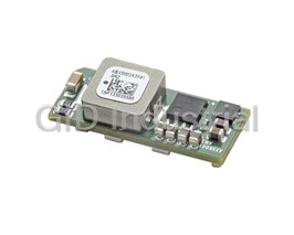
GE CRITICAL POWER QRW025A0F1-HZ

Description
Module DC-DC 48VIN 1-OUT 3.3V 25A 10-Pin Quarter-Brick
Part Number
QRW025A0F1-HZ
Price
Request Quote
Manufacturer
GE CRITICAL POWER
Lead Time
Request Quote
Category
Capacitors » DC-DC Converter
Specifications
Manufacturer
GE Critical Power
Manufacturers Part #
QRW025A0F1-HZ
Industry Aliases
QRW025A0F1-HZ, CC109153053
Brand
GE Critical Power
Series
QRW025
Factory Pack Quantity
36
Cooling Method
Convection
Dimensions
2.28 x 1.45 x 0.38"
Efficiency
85%
Input Type
DC
Input Voltage Nominal
48 VDC
Isolation
1500 VDC
Mechanical Style
Isolated
Mounting
Through Hole
Operating Temperature
- 40 to + 85°C
Output Amps 1
25 A
Package Type
Open Frame
Subcategory
DC-DC Converter
Datasheet

Extracted Text
Data Sheet August 23, 2010 QRW025 Series Power Modules; dc-dc Converters 36Vdc - 75Vdc Input; 1.2 to 3.3 Vdc Output; 25A Features RoHS Compliant Compliant to RoHS EU Directive 2002/95/EC (-Z versions) Compliant to ROHS EU Directive 2002/95/EC with lead solder exemption (non-Z versions) Delivers up to 25A output current Ultra High efficiency – 91% at 3.3V full load Industry standard DOSA Compliant Quarter brick: 57.9 mm x 36.8 mm x 9.5 mm (2.28 in x 1.45 in x 0.375 in) Improved Thermal Performance: 25A at 70ºC at 1m/s (200LFM) for 3.3Vo High power density Applications Low output ripple and noise Enterprise Networks Low output voltages down to 1V: Supports migration to future IC and microprocessor supply voltages Wireless Networks 2:1 input voltage Access and Optical Network Equipment Remote Sense Enterprise Networks Remote On/Off Latest generation IC’s (DSP, FPGA, ASIC) and Constant switching frequency Microprocessor-powered applications. Output overvoltage and Overcurrent protection Options Overtemperature protection Positive Remote On/Off logic Adjustable output voltage (+10% / -20%) Case ground pin (-H Base plate version) Meets the voltage isolation requirements for ETSI 300-132-2 and complies with and is licensed Auto restart after fault shutdown for Basic Insulation rating per EN60950-1 † UL** 60950-1 Recognised, CSA C22.2 No. 60950- ‡ rd 1-03 Certified, and VDE 0805 (IEC60950, 3 Edition) Licensed § CE mark meets 2006/95/EC directive ISO* 9001 certified manufacturing facilities Description The QRW-series dc-dc converters are a new generation of DC/DC power modules designed for optimum efficiency and power density. The QRW series provide up to 25A output current in an industry standard quarter brick, which makes it an ideal choice for small space, high current and low voltage applications. The converter uses synchronous rectification technology and innovative packaging techniques to achieve high efficiency reaching 91% at 3.3V full load. Thanks to the ultra high efficiency of this converter, the power dissipation is such that for most applications a heat sink is not required. In addition, the QRW-series supports future migration of semiconductor and microprocessor supply voltages down to 1.0V. * ISO is a registered trademark of the International Organization of Standards PDF name: QRW025_Series.pdf ** UL is a registered trademark of Underwriters Laboratories, Inc. † CSA is a registered trademark of Canadian Standards Association. ‡ VDE is a trademark of Verband Deutscher Elektrotechniker e.V. § This product is intended for integration into end-use equipment. All of the required procedures of end-use equipment should be followed. QRW025 Series Power Modules; dc-dc Converters Data Sheet 36 Vdc - 75 Vdc Input, 1.2 to 3.3 Vdc Output; 25A August 23, 2010 Absolute Maximum Ratings Stresses in excess of the absolute maximum ratings can cause permanent damage to the device. These are absolute stress ratings only, functional operation of the device is not implied at these or any other conditions in excess of those given in the operations sections of the data sheet. Exposure to absolute maximum ratings for extended periods can adversely affect the device reliabiltiy. Parameter Device Symbol Min Max Unit Input Voltage:Continuous All VI — 75 Vdc Transient (100ms) VI, trans — 100 Vdc Operating Ambient Temperature All TA –40 85 °C (See Thermal Considerations section) Storage Temperature All Tstg –55 125 °C I/O Isolation Voltage (100% factory Hi-Pot tested) — — — 1500 Vdc When using optional case ground pin 700 Vdc (option 7) Electrical Specifications Unless otherwise indicated, specifications apply over all operating input voltage, resistive load, and temperature conditions. Parameter Device Symbol Min Typ Max Unit Operating Input Voltage All VIN 36 48 75 Vdc Maximum Input Current All — — 2.8m n Adc (VI = 0 V to 75 V; IO = IO, max) 2 2 Inrush Transient All It1A s Input Reflected Ripple Current, peak-peak All 16 mAp-p (5 Hz to 20 MHz, 12 µH source impedance See Test configuration section) Input Ripple Rejection (120 Hz) All 60 dB CAUTION: This power module is not internally fused. An input line fuse must always be used. This power module can be used in a wide variety of applications, ranging from simple stand-alone operation to an integrated part of a sophisticated power architecture. To preserve maximum flexibility, internal fusing is not included; however, to achieve maximum safety and system protection, always use an input line fuse. The safety agencies require a normal-blow fuse with a maximum rating of 10 A (see Safety Considerations section). Based on the information provided in this data sheet on inrush energy and maximum dc input current, the same type of fuse with a lower rating can be used. Refer to the fuse manufacturer’s data for further information. Lineage Power 2 QRW025 Series Power Modules; dc-dc Converters Data Sheet 36 Vdc - 75 Vdc Input, 1.2 to 3.3 Vdc Output; 25A August 23, 2010 Electrical Specifications (continued) Output Specifications for the QRW025A0P (Vo = 1.2Vdc) Parameter Device Symbol Min Typ Max Unit Output Voltage Set Point P Vo 1.18 1.2 1.22 Vdc (VI = 48 Vdc; IO = IO, min to IO, max, TA = 25 °C) Output Voltage P Vo 1.15 — 1.25 Vdc (Over all operating input voltage, resistive load, and temperature conditions at steady state until end of life.) Output Regulation: Line (VI = VI, min to VI, max) P— — 0.05 0.3 %, VO, set Load (IO = IO, min to IO, max) — — 0.05 0.3 %, VO, set Temperature (TA = TA, min to TA, max) — — 5 20 mV Output Ripple and Noise RMS (5 Hz to 20 MHz bandwidth) P— — 30 mVrms Peak-to-peak (5 Hz to 20 MHz bandwidth) — — 100 mVp-p External Load Capacitance — 25,000 µF Output Current PIO 0.0—25 Adc (Vo =90% of VO, nom.) Output Current-limit Inception P IO, lim — 29 — Adc (VO = 90% of VO, set) Output Short-circuit Current (Average)VO = 0.25 V Latched off Efficiency η —85 — % (VI = VIN, nom; IO = IO, max), TA = 25 °C Switching Frequency All fSW — 300 — kHz Dynamic Response (ΔIO/Δt = 1 A/10 µs, VI = 48 V, TA = 25 °C); tested with a 220 µF aluminium and a 1.0 µf ceramic capacitor across the load.): Load Change from IO = 50% to 75% of IO, max: Peak Deviation 8 mV Settling Time 200 µs (VO < 10% of peak deviation) Load Change from IO = 50% to 25% of IO, max : Peak Deviation 8 mV Settling Time 200 µs (VO < 10% of peak deviation) Isolation Specifications Parameter Symbol Min Typ Max Unit Isolation Capacitance Ciso — 5600 — PF Isolation Resistance Riso 10 — — MW General Specifications Parameter Min Typ Max Unit Calculated MTBF (IO = 80% of IO, max TA = 40 °C) 1,771,000 Hours Weight — 37(1.31) — g (oz.) Lineage Power 3 QRW025 Series Power Modules; dc-dc Converters Data Sheet 36 Vdc - 75 Vdc Input, 1.2 to 3.3 Vdc Output; 25A August 23, 2010 Feature Specifications Unless otherwise indicated, specifications apply over all operating input voltage, resistive load, and temperature conditions. See Feature Descriptions for additional information. Parameter Symbol Min Typ Max Unit Remote On/Off Signal Interface* (VI = 0 V to 75 V; open collector or equivalent compatible; signal referenced to VI(–) terminal; see Figure 34 and Feature Descriptions.): Preferred Logic: Logic Low—Module On Logic High—Module Off Optional Logic: Logic Low—Module Off Logic High—Module On Logic Low: At Ion/off = 1.0 mA At Von/off = 0.0 V Von/off 0 — 1.2 V Logic High: Ion/off — — 1.0 mA At Ion/off = 0.0 µA Leakage Current Von/off — — 15 V Turn-on Time; see Typical Start-up Curve(IO = IO max; Ion/off — — 50 µA Vo within ±1% of steady state) 2 4 ms Output Voltage Adjustment (See Feature Descriptions): Output Voltage Remote-sense Range — — — 10 %VO,rated Output Voltage Set-point Adjustment Range (trim) — 80 — 110 %V0,nom Output Overvoltage Protection VO, ovsd 1.42 — 1.58 V OvertemperaWuUe Protection (IO = IO, max) Tref1 — 127 — °C Lineage Power 4 QRW025 Series Power Modules; dc-dc Converters Data Sheet 36 Vdc - 75 Vdc Input, 1.2 to 3.3 Vdc Output; 25A March 27, 2008 Characteristic Curves The following figures provide typical characteristics curves for the QRW025A0P (VO = 1.2 V) module at room temperature (TA = 25 °C).The figures are identical for both on/off configurations. 1.2 1 IO = 25A 0.8 0.6 IO = 12.5A 0.4 IO = 2.5A 0.2 TIME, t, (.2 µs/div) 0 0 1020304050607080 Tested with a 220µF aluminium and a 1.0µF ceramic INPUT VOLTAGE, VI (V) capacitor across the load. Figure 1. Input Voltage and Current Characteristics. Figure 4. Transient Response to Step decrease in Load from 50% to 25% of Full Load (VI = 48 100 Vdc). 90 80 70 60 VI = 75V 50 VI = 48V VI = 36V 40 30 20 10 0 0 5 10 15 20 25 30 OUTPUT CURRENT, IO (A) TIME, t, (.2 µs/div) Figure 2. Converter Efficiency vs. Output Current. Figure 5. Transient Response to Step Increase in Load from 50% to 75% of Full Load (VI = 48 Vdc). 36V, 25A 48V, 25A 75V, 25A TIME, t (1 µs/div) Figure 6. Start-up from Remote On/Off (IO = IO, max). Figure 3. Output Ripple Voltage (IO = IO, max). Lineage Power 5 OUTPUT VOLTAGE, VO (V) (20 mV/div) INPUT CURRENT, II (A) OUTPUT CURRENT, IO (A) OUTPUT VOLTAGE, VO (V) OUTPUT CURRENT, IO (A) OUTPUT VOLTAGE, VO (V) (5 A/div) (50 mV/div) 0.5 (5 A/div) (50 mV/div) EFFICIENCY, η (%) QRW025 Series Power Modules; dc-dc Converters Data Sheet 36 Vdc - 75 Vdc Input, 1.2 to 3.3 Vdc Output; 25A August 23, 2010 Electrical Specifications (continued) Output Specifications for the QRW025AOM (Vo = 1.5Vdc) Parameter Device Symbol Min Typ Max Unit Output Voltage Set Point MVo1.471.51.52Vdc (VI = 48 Vdc; IO = IO, min to IO, max, TA = 25 °C) Output Voltage MVo1.45—1.55Vdc (Over all operating input voltage, resistive load, and temperature conditions at steady state until end of life.) Output Regulation: Line (VI = VI, min to VI, max) M— — 0.05 0.2 %, VO, set Load (IO = IO, min to IO, max) — — 0.05 0.2 %, VO, set Temperature (TA = TA, min to TA, max) — — 15 50 mV Output Ripple and Noise RMS (5 Hz to 20 MHz bandwidth) M— — 20 mVrms Peak-to-peak (5 Hz to 20 MHz bandwidth) — — 100 mVp-p External Load Capacitance — 25,000 µF Output Current MIO 0.0—25 Adc (Vo =90% of VO, nom.) Output Current-limit Inception M IO, lim — 30 — Adc (VO = 90% of VO, set) Output Short-circuit Current (Average)VO = 0.25 V Latched off Efficiency η —87— % (VI = VIN, nom; IO = IO, max), TA = 25 °C Switching Frequency All fSW — 300 — kHz Dynamic Response (DIO/Dt = 1 A/10 µs, VI = 48 V, TA = 25 °C); tested with a 220 µF aluminium and a 1.0 µf ceramic capacitor across the load.): Load Change from IO = 50% to 75% of IO, max: Peak Deviation 6 mV Settling Time 200 µs (VO < 10% of peak deviation) Load Change from IO = 50% to 25% of IO, max : 6 Peak Deviation 200 mV Settling Time µs (VO < 10% of peak deviation) Isolation Specifications Parameter Symbol Min Typ Max Unit Isolation Capacitance Ciso — 5600 — PF Isolation Resistance Riso 10 — — MW General Specifications Parameter Min Typ Max Unit Calculated MTBF (IO = 80% of IO, max TA = 40 °C) 1,715,000 Hours Weight — 37(1.31) — g (oz.) Lineage Power 6 QRW025 Series Power Modules; dc-dc Converters Data Sheet 36 Vdc - 75 Vdc Input, 1.2 to 3.3 Vdc Output; 25A August 23, 2010 Feature Specifications Unless otherwise indicated, specifications apply over all operating input voltage, resistive load, and temperature conditions. See Feature Descriptions for additional information. Parameter Symbol Min Typ Max Unit Remote On/Off Signal Interface* (VI = 0 V to 75 V; open collector or equivalent compatible; signal referenced to VI(–) terminal; see Figure 34 and Feature Descriptions.): Preferred Logic: Logic Low—Module On Logic High—Module Off Optional Logic: Logic Low—Module Off Logic High—Module On Logic Low: At Ion/off = 1.0 mA At Von/off = 0.0 V Von/off 0 — 1.2 V Logic High: Ion/off — — 1.0 mA At Ion/off = 0.0 µA Leakage Current Von/off — — 15 V Turn-on Time; see Typical Start-up Curve(IO = IO max; Ion/off — — 50 µA Vo within ±1% of steady state) 2 4 ms Output Voltage Adjustment (See Feature Descriptions): Output Voltage Remote-sense Range — — — 10 %VO,rated Output Voltage Set-point Adjustment Range (trim) — 80 — 110 %V0,nom Output Overvoltage Protection VO, ovsd 1.69 — 2.07 V OvertemperaWuUe Protection (IO = IO, max) Tref1 — 127 — °C * A Minimum OFF Period of 1 sec is recommended. Lineage Power 7 QRW025 Series Power Modules; dc-dc Converters Data Sheet 36 Vdc - 75 Vdc Input, 1.2 to 3.3 Vdc Output; 25A August 23, 2010 Characteristic Curves The following figures provide typical characteristics curves for the QRW025A0M (VO = 1.5 V) module at room temperature (TA = 25 °C) 1.4 1.2 1 IO = 25 A 0.8 0.6 IO = 12.5 A 0.4 0.2 IO = 0 A 0 25 35 45 55 65 75 INPUT VOLTAGE, VI (V) TIME, t (50 µs/div) Tested with a 220µF aluminium and a 1.0µF ceramic capacitor across the load. Figure 7. Input Voltage and Current Characteristics. Figure 10. Transient Response to Step Decrease in Load from 50% to 25% of Full Load (VI = 48 Vdc). 90 88 86 84 82 80 78 VI = 36 V 76 VI = 48 V VI = 75 V 74 72 70 0 5 10 15 20 25 OUTPUT CURRENT, IO (A) Figure 8. Converter Efficiency vs. Output Current. TIME, t (50 µs/div) Figure 11. Transient Response to Step Increase in Load from 50% to 75% of Full Load (VI = 48 Vdc). 36V, 25A 48V, 25A 75V, 25A TIME, t (1 µs/div) Tested with a 10µF aluminium and a 1.0µF tantalum capacitor Figure 9. Output Ripple Voltage (IO = IO, max). across the load. Figure 12. Start-up from Remote On/Off (IO = IO, max). Lineage Power 8 EFFICIENCY η (%) INPUT CURRENT, II (A) OUTPUT VOLTAGE, VO (V) (20 mV/idv) OUTPUT CURRENT, OUTPUT VOLTAGE, OUTPUT CURRENT, OUTPUT VOLTAGE, IO (A) (5 A/div) VO (V) (100 mV/idv) 0. IO (A) (5 A/div) VO (V) (100 mV/idv) QRW025 Series Power Modules; dc-dc Converters Data Sheet 36 Vdc - 75 Vdc Input, 1.2 to 3.3 Vdc Output; 25A August 23, 2010 Electrical Specifications (continued) Output Specifications for the QRW025A0Y (Vo = 1.8Vdc) Parameter Device Symbol Min Typ Max Unit Output Voltage Set Point Y Vo 1.77 1.8 1.83 Vdc (VI = 48 Vdc; IO = IO, min to IO, max, TA = 25 °C) Output Voltage Y Vo 1.75 — 1.85 Vdc (Over all operating input voltage, resistive load, and temperature conditions at steady state until end of life.) Output Regulation: Line (VI = VI, min to VI, max) Y— — 0.05 0.2 %, VO, set Load (IO = IO, min to IO, max) — — 0.05 0.2 %, VO, set Temperature (TA = TA, min to TA, max) — — 15 50 mV Output Ripple and Noise RMS (5 Hz to 20 MHz bandwidth) Y— — 35 mVrms Peak-to-peak (5 Hz to 20 MHz bandwidth) — — 100 mVp-p External Load Capacitance — 25,000 µF Output Current YIO 0.0—25 Adc (Vo =90% of VO, nom.) Output Current-limit Inception Y IO, lim — 30 — Adc (VO = 90% of VO, set) Output Short-circuit Current (Average)VO = 0.25 V Latched off Efficiency η —88 — % (VI = VIN, nom; IO = IO, max), TA = 25 °C Switching Frequency All fSW — 300 — kHz Dynamic Response (DIO/Dt = 1 A/10 µs, VI = 48 V, TA = 25 °C); tested with a 220 µF aluminium and a 1.0 µf ceramic capacitor across the load.): Load Change from IO = 50% to 75% of IO, max: Peak Deviation 8 mV Settling Time 200 µs (VO < 10% of peak deviation) Load Change from IO = 50% to 25% of IO, max : 8 Peak Deviation 200 mV Settling Time µs (VO < 10% of peak deviation) Isolation Specifications Parameter Symbol Min Typ Max Unit Isolation Capacitance Ciso — 5600 — PF Isolation Resistance Riso 10 — — MW General Specifications Parameter Min Typ Max Unit Calculated MTBF (IO = 80% of IO, max TA = 40 °C) 1,644,000 Hours Weight — 37(1.31) — g (oz.) Lineage Power 9 QRW025 Series Power Modules; dc-dc Converters Data Sheet 36 Vdc - 75 Vdc Input, 1.2 to 3.3 Vdc Output; 25A August 23, 2010 Feature Specifications Unless otherwise indicated, specifications apply over all operating input voltage, resistive load, and temperature conditions. See Feature Descriptions for additional information. Parameter Symbol Min Typ Max Unit Remote On/Off Signal Interface* (VI = 0 V to 75 V; open collector or equivalent compatible; signal referenced to VI(–) terminal; see Figure 34 and Feature Descriptions.): Preferred Logic: Logic Low—Module On Logic High—Module Off Optional Logic: Logic Low—Module Off Logic High—Module On Logic Low: At Ion/off = 1.0 mA At Von/off = 0.0 V Von/off 0 — 1.2 V Logic High: Ion/off — — 1.0 mA At Ion/off = 0.0 µA Leakage Current Von/off — — 15 V Turn-on Time; see Typical Start-up Curve(IO = IO max; Ion/off — — 50 µA Vo within ±1% of steady state) 4 8 ms Output Voltage Adjustment (See Feature Descriptions): Output Voltage Remote-sense Range — — — 10 %VO,rated Output Voltage Set-point Adjustment Range (trim) — 80 — 110 %V0,nom Output Overvoltage Protection VO, ovsd 2.0 — 2.5 V OvertemperaWuUe Protection (IO = IO, max) Tref1 — 127 — °C * A Minimum OFF Period of 1 sec is recommended. Lineage Power 10 QRW025 Series Power Modules; dc-dc Converters Data Sheet 36 Vdc - 75 Vdc Input, 1.2 to 3.3 Vdc Output; 25A August 23, 2010 Characteristic Curves The following figures provide typical characteristics curves for the QRW025A0Y (VO = 1.8 V) module at room temperature (TA = 25 °C) 1.6 1.4 IO = 25 A IO = 12.5 A 1.2 IO = 0 A 1 0.8 0.6 0.4 0.2 0 25 30 35 40 45 50 55 60 65 70 75 TIME, t (100 µs/div) INPUT VOLTAGE, VI (V) Tested with a 220µF aluminium and a 1.0µF ceramic capacitor across the load. Figure 13. Input Voltage and Current Characteristics. Figure 16. Transient Response to Step Decrease in Load from 50% to 25% of Full Load (VI = 48 Vdc). 90 88 VI = 36 V 86 84 82 80 78 VI = 75 V 76 VI = 48 V 74 72 70 0 5 10 15 20 25 OUTPUT CURRENT, IO (A) TIME, t (100 µs/div) Figure 14. Converter Efficiency vs. Output Current. Figure 17. Transient Response to Step Increase in Load from 50% to 75% of Full Load (VI = 48 Vdc). VI = 36 V VI = 48 V VI = 75 V TIME, t (2 ms/div) TIME, t (1 µs/div) Tested with a 10µF aluminium and a 1.0µF tantalum capacitor across the load. Figure 15. Output Ripple Voltage (IO = IO, max). Figure 18. Start-up from Remote On/Off (IO = IO, max). Lineage Power 11 EFFICENCY, η (%) INPUT CURRENT, II (A) OUTPUT VOLTAGE, VO (V) (50 mV/div) REMOTE ON/OFF, OUTPUT VOLTAGE, (V) OUTPUT CURRENT, IO (A) OUTPUT VOLTAGE, VO (V) OUTPUT CURRENT, IO (A) OUTPUT VOLTAGE, VO (V) VON/OFF (V) (0.5 V/div) (10 A/div) (100 mV/div) (10 A/div) (100 mV/div) QRW025 Series Power Modules; dc-dc Converters Data Sheet 36 Vdc - 75 Vdc Input, 1.2 to 3.3 Vdc Output; 25A August 23, 2010 Electrical Specifications (continued) Output Specifications for the QRW025A0G (Vo = 2.5Vdc) Parameter Device Symbol Min Typ Max Unit Output Voltage Set Point G Vo 2.47 2.5 2.53 Vdc (VI = 48 Vdc; IO = IO, min to IO, max, TA = 25 °C) Output Voltage G Vo 2.42 — 2.58 Vdc (Over all operating input voltage, resistive load, and temperature conditions at steady state until end of life.) Output Regulation: Line (VI = VI, min to VI, max) G— — 0.05 0.2 %, VO, set Load (IO = IO, min to IO, max) — — 0.05 0.2 %, VO, set Temperature (TA = TA, min to TA, max) — — 15 50 mV Output Ripple and Noise RMS (5 Hz to 20 MHz bandwidth) G— — 35 mVrms Peak-to-peak (5 Hz to 20 MHz bandwidth) — — 100 mVp-p External Load Capacitance — 25,000 µF Output Current GIO 0.0—25 Adc (Vo =90% of VO, nom.) Output Current-limit Inception G IO, lim — 30 — Adc (VO = 90% of VO, set) Output Short-circuit Current (Average)VO = 0.25 V Latched off Efficiency η —90 — % (VI = VIN, nom; IO = IO, max), TA = 25 °C Switching Frequency All fSW — 300 — kHz Dynamic Response (DIO/Dt = 1 A/10 µs, VI = 48 V, TA = 25 °C); tested with a 220 µF aluminium and a 1.0 µf ceramic capacitor across the load.): Load Change from IO = 50% to 75% of IO, max: Peak Deviation 5 mV Settling Time 200 µs (VO < 10% of peak deviation) Load Change from IO = 50% to 25% of IO, max : 5 Peak Deviation 200 mV Settling Time µs (VO < 10% of peak deviation) Isolation Specifications Parameter Symbol Min Typ Max Unit Isolation Capacitance Ciso — 5600 — PF Isolation Resistance Riso 10 — — MW General Specifications Parameter Min Typ Max Unit Calculated MTBF (IO = 80% of IO, max TA = 40 °C) 1,558,000 Hours Weight — 37(1.31) — g (oz.) Lineage Power 12 QRW025 Series Power Modules; dc-dc Converters Data Sheet 36 Vdc - 75 Vdc Input, 1.2 to 3.3 Vdc Output; 25A August 23, 2010 Feature Specifications Unless otherwise indicated, specifications apply over all operating input voltage, resistive load, and temperature conditions. See Feature Descriptions for additional information. Parameter Symbol Min Typ Max Unit Remote On/Off Signal Interface* (VI = 0 V to 75 V; open collector or equivalent compatible; signal referenced to VI(–) terminal; see Figure 52 and Feature Descriptions.): Preferred Logic: Logic Low—Module On Logic High—Module Off Optional Logic: Logic Low—Module Off Logic High—Module On Logic Low: At Ion/off = 1.0 mA At Von/off = 0.0 V Von/off 0 — 1.2 V Logic High: Ion/off — — 1.0 mA At Ion/off = 0.0 µA Leakage Current Von/off — — 15 V Turn-on Time; see Typical Start-up Curve(IO = IO max; Ion/off — — 50 µA Vo within ±1% of steady state) 2 4 ms Output Voltage Adjustment (See Feature Descriptions): Output Voltage Remote-sense Range — — — 10 %VO,rated Output Voltage Set-point Adjustment Range (trim) — 80 — 110 %V0,nom Output Overvoltage Protection VO, ovsd 2.9 — 3.2 V OvertemperaWuUe Protection (IO = IO, max) Tref1 — 127 — °C * A Minimum OFF Period of 1 sec is recommended. Lineage Power 13 QRW025 Series Power Modules; dc-dc Converters Data Sheet 36 Vdc - 75 Vdc Input, 1.2 to 3.3 Vdc Output; 25A August 23, 2010 Characteristic Curves The following figures provide typical characteristics curves for the QRW025A0G (VO = 2.5 V) module at room temperature (TA = 25 °C) 2 1.8 1.6 1.4 1.2 IO = 25 A 1 0.8 IO = 12.5 A 0.6 0.4 0.2 IO = 0 A 0 25 35 45 55 65 75 TIME, t (100 µs/div) INPUT VOLTAGE, VI (V) Tested with a 220µF aluminium and a 1.0µF ceramic capacitor across the load. Figure 22. Transient Response to Step Decrease in Figure 19. Input Voltage and Current Characteristics. Load from 50% to 25% of Full Load (VI = 48 Vdc). 95 VI = 36 V 90 85 80 VI = 48 V VI = 75 V 75 70 0 5 10 15 20 25 OUTPUT CURRENT, IO (A) TIME, t (100 µs/div) Figure 23. Transient Response to Step Increase in Figure 20. Converter Efficiency vs. Output Current. Load from 50% to 75% of Full Load (VI = 48 Vdc). TIME, t (1 ms/div) TIME, t (1 µs/div) Tested with a 10µF aluminium and a 1.0µF tantalum capacitor across the load. Figure 21. Output Ripple Voltage (IO = IO, max). Figure 24. Start-up from Remote On/Off (IO = IO, max). Lineage Power 14 EFFICIENCY η (%) INPUT CURRENT, II (A) OUTPUT VOLTAGE, VO (V) (50 mV/div) REMOTE ON/OFF, OUTPUT VOLTAGE, VO (V) OUTPUT CURRENT, IO (A) OUTPUT VOLTAGE, VO (V) Von/off (V) (1 V/div) (5 A/div) (100 mV/div) OUTPUT CURRENT, IO (A) OUTPUT VOLTAGE, VO (V) (5 A/div) (100 mV/div) QRW025 Series Power Modules; dc-dc Converters Data Sheet 36 Vdc - 75 Vdc Input, 1.2 to 3.3 Vdc Output; 25A August 23, 2010 Electrical Specifications (continued) Output Specifications for the QRW025A0F (Vo = 3.3Vdc) Parameter Device Symbol Min Typ Max Unit Output Voltage Set Point F Vo 3.24 3.3 3.36 Vdc (VI = 48 Vdc; IO = IO, min to IO, max, TA = 25 °C) Output Voltage F Vo 3.2 — 3.4 Vdc (Over all operating input voltage, resistive load, and temperature conditions at steady state until end of life.) Output Regulation: Line (VI = VI, min to VI, max) F— — 0.05 0.2 %, VO, set Load (IO = IO, min to IO, max) — — 0.05 0.2 %, VO, set Temperature (TA = TA, min to TA, max) — — 15 50 mV Output Ripple and Noise RMS (5 Hz to 20 MHz bandwidth) F— — 30 mVrms Peak-to-peak (5 Hz to 20 MHz bandwidth) — — 100 mVp-p External Load Capacitance — 30,000 µF Output Current FIO 0.0—25 Adc (Vo =90% of VO, nom.) Output Current-limit Inception F IO, lim — 28 — Adc (VO = 90% of VO, set) Output Short-circuit Current (Average)VO = 0.25 V Latched off Efficiency η —91 — % (VI = VIN, nom; IO = IO, max), TA = 25 °C Switching Frequency All fSW — 300 — kHz Dynamic Response (DIO/Dt = 1 A/10 µs, VI = 48 V, TA = 25 °C); tested with a 220 µF aluminium and a 1.0 µf ceramic capacitor across the load.): Load Change from IO = 50% to 75% of IO, max: Peak Deviation 5 mV Settling Time 200 µs (VO < 10% of peak deviation) Load Change from IO = 50% to 25% of IO, max : 5 Peak Deviation 200 mV Settling Time µs (VO < 10% of peak deviation) Isolation Specifications Parameter Symbol Min Typ Max Unit Isolation Capacitance Ciso — 5600 — PF Isolation Resistance Riso 10 — — MW General Specifications Parameter Min Typ Max Unit Calculated MTBF (IO = 80% of IO, max TA = 40 °C) 1,548,000 Hours Weight — 37(1.31) — g (oz.) Lineage Power 15 QRW025 Series Power Modules; dc-dc Converters Data Sheet 36 Vdc - 75 Vdc Input, 1.2 to 3.3 Vdc Output; 25A August 23, 2010 Feature Specifications Unless otherwise indicated, specifications apply over all operating input voltage, resistive load, and temperature conditions. See Feature Descriptions for additional information. Parameter Symbol Min Typ Max Unit Remote On/Off Signal Interface* (VI = 0 V to 75 V; open collector or equivalent compatible; signal referenced to VI(–) terminal; see Figure 34 and Feature Descriptions.): Preferred Logic: Logic Low—Module On Logic High—Module Off Optional Logic: Logic Low—Module Off Logic High—Module On Logic Low: At Ion/off = 1.0 mA At Von/off = 0.0 V Von/off 0 — 1.2 V Logic High: Ion/off — — 1.0 mA At Ion/off = 0.0 µA Leakage Current Von/off — — 15 V Turn-on Time; see Typical Start-up Curve(IO = IO max; Ion/off — — 50 µA Vo within ±1% of steady state) 2 4 ms Output Voltage Adjustment (See Feature Descriptions): Output Voltage Remote-sense Range — — — 10 %V0,nom Output Voltage Set-point Adjustment Range (trim) — 80 — 110 %V0,nom Output Overvoltage Protection VO, ovsd 3.8 — 4.6 V OvertemperaWuUe Protection (IO = IO, max) Tref1 — 127 — °C * A Minimum OFF Period of 1 sec is recommended. Lineage Power 16 QRW025 Series Power Modules; dc-dc Converters Data Sheet 36 Vdc - 75 Vdc Input, 1.2 to 3.3 Vdc Output; 25A August 23, 2010 Characteristic Curves The following figures provide typical characteristics curves for the QRW025A0F (VO = 3.3 V) module at room temperature (TA = 25 °C) 3.5 3 IO = 25 A IO = 12.5 A IO = 2.5 A 2.5 2 1.5 1 0.5 0 0 10 20304050 6070 INPUT VOLTAGE, VI (V) Tested with a 220µF aluminium and a 1.0µF ceramic capacitor across the load. Figure 25. Input Voltage and Current Characteristics. Figure 28. Transient Response to Step Decrease in Load from 50% to 25% of Full Load (VI = 48 Vdc). 95 90 85 VI = 36 V 80 VI = 48 V V = 75 V I 75 70 0 5 10 15 20 25 30 OUTPUT CURRENT, IO (A) Figure 29. Transient Response to Step Increase in Load Figure 26. Converter Efficiency vs. Output Current. from 50% to 75% of Full Load (VI = 48 Vdc). 36V, 25A 48V, 25A 75V, 25A TIME, t (2 ms/div) TIME, t (2µs/div) Tested with a 10µF aluminium and a 1.0µF tantalum capacitor across the load. Figure 27. Output Ripple Voltage (IO = IO, max). Figure 30. Start-up from Remote On/Off (IO = IO, max). Lineage Power 17 EFFICENCY, η (%) OUTPUT VOLTAGE, VO (V) (50 mV/div) INPUT CURRENT, II (A) OUTPUT VOLTAGE (V) REMOTE ON/OFF (1 V/div) VON/OFF (V) QRW025 Series Power Modules; dc-dc Converters Data Sheet 36 Vdc - 75 Vdc Input, 1.2 to 3.3 Vdc Output; 25A August 23, 2010 Test Configurations Design Considerations TO Input Source Impedance OSCILLOSCOPE CURRENT LTEST PROBE The power module should be connected to a low VI(+) 12 μH ac-impedance input source. Highly inductive source imped- CS 220 μF ances can affect the stability of the power BATTERY ESR < 0.1 Ω module. For the test configuration in 31, @ 20 ºC 100 kHz a 33 µF electrolytic capacitor (ESR < 0.7 W at 100 kHz) mounted close to the power module helps ensure VI(–) stability of the unit. For other highly inductive source imped- ances, consult the factory for further application guidelines. Note:Measure input reflected-ripple current with a simulated source inductance (LTEST) of 12 µH. Capacitor CS off- Output Capacitance sets possible battery impedance. Measure current as shown above. High output current transient rate of change (high di/dt) loads Figure 31. Input Reflected-Ripple Test Setup. may require high values of output capacitance to supply the instantaneous energy requirement to the load. Tp minimize the output voltage transient drop COPPER STRIPS during this transient, low E.S.R. (equivalent series resistance) capacitors may be required, since a high E.S.R. will produce VO(+) a correspondingly higher voltage drop during the current tran- sient. 1.0 μF 10 μF RESISTIVE SCOPE LOAD Output capacitance and load impedance interact with the power module’s output voltage regulation control system and VO(-) may produce an ’unstable’ output condition for the required values of capacitance and E.S.R.. Minimum and maximum values of output capacitance and of the capacitor’s associ- ated E.S.R. may be dictated, depending on the module’s con- Note:Use a 1.0 µF ceramic capacitor and a 10 µF aluminum trol system. or tantalum capacitor. Scope measurement should be made using a BNC socket. Position the load between The process of determining the acceptable values of capaci- 51 mm and 76 mm (2 in. and 3 in.) from the module. tance and E.S.R. is complex and is load-dependant. Lineage provides Web-based tools to assist the power module end- user in appraising and adjusting the effect of various load Figure 32. Peak-to-Peak Output Noise Measurement Test conditions and output capacitances on specific power mod- Setup. ules for various load conditions. CONTACT AND Safety Considerations SENSE(+) DISTRIBUTION LOSSES VI(+) VO(+) For safety-agency approval of the system in which the power IO II module is used, the power module must be installed in com- SUPPLY LOAD pliance with the spacing and separation requirements of the end-use safety agency standard, i.e., UL60950, CSA C22.2 VI(–) VO(–) No. 60950-00, and VDE 0805:2001-12 (IEC60950, 3rd Ed). CONTACT SENSE(–) RESISTANCE These converters have been evaluated to the spacing requirements for Basic Insulation, per the above safety stan- dards; and 1500 Vdc is applied from VI to VO to 100% of out- Note:All measurements are taken at the module terminals. going production. When socketing, place Kelvin connections at module terminals to avoid measurement errors due to socket For end products connected to –48 Vdc, or –60 Vdc nomianl contact resistance. DC MAINS (i.e. central office dc battery plant), no further fault testing is required. [] V (+) – V (-) I Note:–60 V dc nominal bettery plants are not available in the O O O ⎛⎞ η = --- ---- ---- --- ---- ---- ---- --- ---- ---- ---- ---- - × 100 % U.S. or Canada. ⎝⎠ [] V (+) – V (-) I I I I For all input voltages, other than DC MAINS, where the input voltage is less than 60 Vdc, if the input meets all of the Figure 33. Output Voltage and Efficiency Measurement. requirements for SELV, then: n The output may be considered SELV. Output voltages will Lineage Power 18 QRW025 Series Power Modules; dc-dc Converters Data Sheet 36 Vdc - 75 Vdc Input, 1.2 to 3.3 Vdc Output; 25A August 23, 2010 remain withing SELV limits even with internally-generated non-SELV voltages. Single component failure and fault tests were performed in the power converters. n One pole of the input and one pole of the output are to be grounded, or both circuits are to be kept floating, to main- tain the output voltage to ground voltage within ELV or SELV limits. For all input sources, other than DC MAINS, where the input voltage is between 60 and 75 Vdc (Classified as TNV-2 in Europe), the following must be adhered to, if the converter’s output is to be evaluated for SELV: n The input source is to be provided with reinforced insula- tion from any hazardous voltage, including the AC mains. n One VI pin and one VO pin are to be reliably earthed, or both the input and output pins are to be kept floating. n Another SELV reliability test is conducted on the whole system, as required by the safety agencies, on the combi- nation of supply source and the subject module to verify that under a single fault, hazardous voltages do not appear at the module’s output. The power module has ELV (extra-low voltage) outputs when all inputs are ELV. All flammable materials used in the manufacturing of these modules are rated 94V-0, and UL60950A.2 for reduced thick- nesses. The input to these units is to be provided with a max- imum 10A normal-blow fuse in the ungrounded lead. Lineage Power 19 QRW025 Series Power Modules; dc-dc Converters Data Sheet 36 Vdc - 75 Vdc Input, 1.2 to 3.3 Vdc Output; 25A August 23, 2010 [Vo(+) – Vo(-)] – [SENSE(+) – SENSE(-)] £ 10% of Vo, rated Feature Descriptions The voltage between the Vo(+) and Vo(-) terminals must not Overcurrent Protection exceed the minimum output overvoltage shutdown value indicated in the Feature Specifications table. This limit To provide protection in a fault output overload condition, the includes any increase in voltage due to remote-sense com- module is equipped with internal current-limiting circuitry and pensation and output voltage set-point adjustment (trim). can endure current limit for few seconds. If overcurrent per- See Figure 35. sists for few seconds, the module will shut down and remain If not using the remote-sense feature to regulate the output latch-off. at the point of load, then connect SENSE(+) to Vo(+) and The overcurrent latch is reset by either cycling the input SENSE(-) to Vo(-) at the module. power or by toggling the on/off pin for one second. If the out- Although the output voltage can be increased by both the put overload condition still exists when the module restarts, it remote sense and by tine trim, the maximum increase for the will shut down again. This operation will continue indefinitely output voltage is not the sum of both. The maximum until the overcurrent condition is corrected. increase is the larger of either the remote sense or the trim. An auto-restart option is also available. The amount of power delivered by the module is defined as the voltage at the output terminals multiplied by the output Remote On/Off current. When using remote sense and trim: the output volt- age of the module can be increased, which at the same out- Two remote on/off options are available. Positive logic put current would increase the power output of the module. remote on/off turns the module on during a logic-high volt- Care should be taken to ensure that the maximum output age on the ON/OFF pin, and off during a logic low. Negative power of the module remains at or below the maximum rated logic remote on/off turns the module off during a logic high power. and on during a logic low. Negative logic, device code suffix "1," is the factory-preferred configuration. To turn the power module on and off, the user must supply a switch to control the voltage between the on/off terminal and SENSE(+) the VI(-) terminal (Von/off). The switch can be an open col- SENSE(–) lector or equivalent (see Figure 10). A logic low is Von/off = 0 V to I.2 V. The maximum Ion/off during a logic low is 1 mA. VI(+) VO(+) IO The switch should maintain a logic-low voltage while sinking SUPPLY LOAD II 1 mA. VI(–) VO(–) CONTACT CONTACT AND During a logic high, the maximum Von/off generated by the RESISTANCE DISTRIBUTION LOSSES power module is 15 V. The maximum allowable leakage cur- rent of the switch at Von/off = 15V is 50 µA. Figure 35. Effective Circuit Configuration for If not using the remote on/off feature, do one of the following Single-Module Remote-Sense Operation to turn the unit on Output Voltage. For negative logic, short ON/OFF pin to VI(-). Output Overvoltage Protection For positive logic: leave ON/OFF pin open. Ion/off The output overvoltage protection consists of circuitry that ON/OFF + monitors the voltage on the output terminals. If the voltage Von/off SENSE(+) on the output terminals exceeds the over voltage protection – threshold, then the module will shutdown and latch off. The VO(+) LOAD overvoltage latch is reset by either cycling the input power VO(–) for one second or by toggling the on/off signal for one sec- VI(+) ond. SENSE(–) I(–) V The protection mechanism is such that the unit can continue in this condition until the fault is cleared. Figure 34. Remote On/Off Implementation. Overtemperature Protection These modules feature an overtemperature protection circuit Remote Sense to safeguard against thermal damage. The circuit shuts down and latches off the module when the maximum device Remote sense minimizes the effects of distribution losses by reference temperature is exceeded. The module can be regulating the voltage at the remote-sense connections. The restarted by cycling the dc input power for at least one sec- voltage between the remote-sense pins and the output ter- ond or by toggling the remote on/off signal for at least one minals must not exceed the output voltage sense range second. given in the Feature Specifications table i.e.: Lineage Power 20 QRW025 Series Power Modules; dc-dc Converters Data Sheet 36 Vdc - 75 Vdc Input, 1.2 to 3.3 Vdc Output; 25A August 23, 2010 Feature Descriptions (Continued) Output Voltage Set-Point Adjustment (Trim) VI(+) VO(+) Trimming allows the user to increase or decrease the output voltage set point of a module. This is accomplished by con- ON/OFF SENSE(+) necting an external resistor between the TRIM pin and either the SENSE(+) or SENSE(-) pins. The trim resistor should be CASE TRIM RLOAD positioned close to the module. Radj-down VI(–) SENSE(–) If not using the trim feature, leave the TRIM pin open. With an external resistor between the TRIM and SENSE(-) VO(–) pins (Radj-down), the output voltage set point (Vo,adj) decreases (see Figure 36). The following equation deter- mines the required external-resistor value to obtain a per- Figure 36. Circuit Configuration to Decrease Output centage output voltage change of Δ%. Voltage. For Output Voltage: 1.2V - 12V VI(+) VO(+) With an external resistor connected between the TRIM and SENSE(+) pins (Radj-up), the output voltage set point ON/OFF SENSE(+) (Vo,adj) increases (see Figure 37). Radj-up CASE TRIM RLOAD The following equation determines the required external- resistor value to obtain a percentage output voltage change VI(–) SENSE(–) of D% For Output Voltage: 1.5V - 12V VO(–) Figure 37. Circuit Configuration to Increase Output Voltage. For Output Voltage: 1.2V The voltage between the Vo(+) and Vo(-) terminals must not exceed the minimum output overvoltage shut-down value indicated in the Feature Specifications table. This limit includes any increase in voltage due to remote-sense com- pensation and output voltage set-point adjustment (trim). See Figure 35. Although the output voltage can be increased by both the remote sense and by the trim, the maximum increase for the output voltage is not the sum of both. The maximum increase is the larger of either the remote sense or the trim. The amount of power delivered by the module is defined as the voltage at the output terminals multiplied by the output current. When using remote sense and trim, the output volt- age of the module can be increased, which at the same out- put current would increase the power output of the module. Care should be taken to ensure that the maximum output power of the module remains at or below the maximum rated power. Lineage Power 21 QRW025 Series Power Modules; dc-dc Converters Data Sheet 36 Vdc - 75 Vdc Input, 1.2 to 3.3 Vdc Output; 25A August 23, 2010 versus local ambient temperature (TA) for natural convection Thermal Considerations through 2 m/s (400 ft./min.). The power modules operate in a variety of thermal environ- Note that the natural convection condition was measured at 0.05 m/s to 0.1 m/s (10ft./min. to 20 ft./min.); however, sys- ments; however, sufficient cooling should be provided to tems in which these power modules may be used typically help ensure reliable operation of the unit. Heat-dissipating generate natural convection airflow rates of 0.3 m/s (60 ft./ components are mounted on the top side of the module. min.) due to other heat dissipating components in the sys- Heat is removed by conduction, convection and radiation to tem. The use of output power derating curve is shown in the the surrounding environment. Proper cooling can be verified following example. by measuring the temperature of selected components on the topside of the power module (See 38). Peak temperature What is the minimum airflow necessary for a QRW025A0F (Tref) can occur at any of these positions indicated in Figure operating at VI = 48 V, an output current of 25A, and a maxi- 50. mum ambient temperature of 70 °C. Solution Given: VI = 48V Io = 25A TA = 70 °C Determine airflow (v) (Use Figure 43): v = 1m/sec. (200ft./min.) 40 35 30 25 20 15 1 10 Note:Top view, pin locations are for reference only. 5 0 Figure 38. Temperature Measurement Location. 20 30 40 50 60 70 80 90 LOCAL AMBIENT TEMPERATURE, TA (°C) Figure 39. Output Power Derating for QRW025A0P (Vo = The temperature at any one of these locations should not 1.2V) in Transverse Orientation with No exceed per Table 1 to ensure reliable operation of the power Baseplate; Airflow direction from VIN (+) to module. The output power of the module should not exceed VIN (–); VIN = 48V. the rated power for the module as listed in the Ordering Information table. 40 Although the maximum Tref temperature of the power mod- 35 ules is per Table 1, you can limit these temperatures to a lower value for extremely high reliability. 30 25 Table 1. Device Temperature 20 Output Voltage Device Temperature (°C) 15 1.2V Tref1 114 1.5V Tref1 111 10 1.8V Tref1 117 5 2.5V Tref1 117 0 3.3V Tref1 117 20 30 40 50 60 70 80 90 LOCAL AMBIENT TEMPERATURE, TA (°C) Heat Transfer Without Heat Sinks Figure 40. Output Power Derating for QRW025A0M (Vo = 1.5V) in Transverse Orientation with No Increasing airflow over the module enhances the heat trans- Baseplate; Airflow direction from VIN (+) to fer via convection. Figures 39 through 43 shows the maxi- VIN (–); VIN = 48V. mum current that can be delivered by the corresponding module without exceeding the maximum case temperature Lineage Power 22 OUTPUT CURRENT, IO (A) OUTPUT CURRENT, IO (A) QRW025 Series Power Modules; dc-dc Converters Data Sheet 36 Vdc - 75 Vdc Input, 1.2 to 3.3 Vdc Output; 25A August 23, 2010 Thermal Considerations (continued) Figure 41. Output Power Derating for QRW025A0Y (Vo = 1.8V) in Transverse Orientation with No Baseplate; Airflow direction from VIN (+) to VIN (–); VIN = 48V. Figure 42. Output Power Derating for QRW025A0G (Vo = 2.5V) in Transverse Orientation with No Baseplate; Airflow direction from VIN (+) to VIN (–); VIN = 48V. 40 35 30 25 20 15 10 5 0 20 30 40 50 60 70 80 90 LOCAL AMBIENT TEMPERATURE, TA (°C) Figure 43. Output Power Derating for QRW025A0F (Vo = 3.3) in Transverse Orientation with No Baseplate; Airflow direction from VIN (+) to VIN (–); VIN = 48V. Lineage Power 23 OUTPUT CURRENT, IO (A) QRW025 Series Power Modules; dc-dc Converters Data Sheet 36 Vdc - 75 Vdc Input, 1.2 to 3.3 Vdc Output; 25A August 23, 2010 Outline Diagram Dimensions are in millimeters and (inches) Tolerences: x.x mm 0.5 mm (x.xx in. 0.02 in.) x.xx mm 0.25 mm (x.xxx in. 0.010 in.) Top View Side View Bottom View *Top Side label includes Lineage name, product designation, and data code. † Optional Features, Pin is not present unless one of these options is specified. Lineage Power 24 QRW025 Series Power Modules; dc-dc Converters Data Sheet 36 Vdc - 75 Vdc Input, 1.2 to 3.3 Vdc Output; 25A August 23, 2010 Recommended Hole Pattern Dimensions are in millimeters and (inches). Lineage Power 25 QRW025 Series Power Modules; dc-dc Converters Data Sheet 36 Vdc - 75 Vdc Input, 1.2 to 3.3 Vdc Output; 25A August 23, 2010 Through-Hole Lead-Free Soldering Infor- mation The RoHS-compliant through-hole products use the SAC (Sn/Ag/Cu) Pb-free solder and RoHS-compliant compo- nents. They are designed to be processed through single or dual wave soldering machines. The pins have an RoHS- compliant finish that is compatible with both Pb and Pb-free wave soldering processes. A maximum preheat rate of 3°C/s is suggested. The wave preheat process should be such that the temperature of the power module board is kept below 210°C. For Pb solder, the recommended pot temper- ature is 260°C, while the Pb-free solder pot is 270°C max. Not all RoHS-compliant through-hole products can be pro- cessed with paste-through-hole Pb or Pb-free reflow pro- cess. If additional information is needed, please consult with your Lineage Power representative for more details. Post Solder Cleaning and Drying Considerations Post solder cleaning is usually the final circuit-board assembly process prior to electrical board testing. The result of inadequate cleaning and drying can affect both the reliability of a power module and the testability of the finished circuit-board assembly. For guidance on appropriate soldering, cleaning and drying procedures, refer to Lineage Power Board Mounted Power Modules: Soldering and Cleaning Application Note (AP01-056EPS). Lineage Power 26 Data Sheet QRW025 Series Power Modules; dc-dc Converters August 23, 2010 36 Vdc - 75 Vdc Input, 1.2 to 3.3 Vdc Output; 25A Ordering Information Please contact your Lineage Power Sales Representative for pricing, availability and optional features. Table 1. Product Codes Output Output Input Voltage Efficiency Connector Type Product Codes Comcodes Voltage Current QRW025A0F1 108965765 48V (36-75Vdc) 3.3V 25A 91% Through hole QRW025A0F4 108974809 48V (36-75Vdc) 3.3V 25A 91% Through hole QRW025A0F41 108969213 48V (36-75Vdc) 3.3V 25A 91% Through hole 48V (36-75Vdc) 3.3V 25A 91% Through hole QRW025A0F1Z CC109101482 QRW025A0F1-H 108968918 48V (36-75Vdc) 3.3V 25A 91% Through hole QRW025A0F41-H 108981267 48V (36-75Vdc) 3.3V 25A 91% Through hole QRW025A0F1-HZ CC109153053 48V (36-75Vdc) 3.3V 25A 91% Through hole QRW025A0G41 108971656 48V (36-75Vdc) 2.5V 25A 90% Through hole 48V (36-75Vdc) 2.5V 25A 90% Through hole QRW025A0G1-H 108972126 QRW025A0Y4 108974825 48V (36-75Vdc) 1.8V 25A 88% Through hole QRW025A0Y61 108975483 48V (36-75Vdc) 1.8V 25A 88% Through hole QRW025A0M41-H 108986373 48V (36-75Vdc) 1.5V 25A 87% Through hole QRW025A0M641-H CC109155297 48V (36-75Vdc) 1.5V 25A 87% Through hole QRW025A0P1 108965799 48V (36-75Vdc) 1.2V 25A 85% Through hole 48V (36-75Vdc) 1.2V 25A 85% Through hole QRW025A0P1Z CC109139515 Table 2. Device Options Character and Position Characteristic Definition Form Factor Q Q = Quarter Brick Family Designator R Family Designator Input Voltage W W = Wide Range, 36V-75V Output Current 025A0 025A0 = 025.0 Amps Maximum Output Current F F =3.3V nominal G G =2.5V nominal Output Voltage Y Y =1.8V nominal M M =1.5V nominal P P =1.2V nominal Omit = Default Pin Length shown in Mechanical Outline Figures 8 8 = Pin Length: 2.79 mm ± 0.25mm , (0.110 in. ± 0.010 in.) Pin Length 7 7 = Case Pin (only available with H option) 6 6 = Pin Length: 3.68 mm ± 0.25mm , (0.145 in. ± 0.010 in.) Action following Omit = Latching Mode Protective Shutdown 4 4 = Auto-restart following shutdown (Overcurrent/Overvoltage) Omit = Positive Logic On/Off Logic 1 1 = Negative Logic Omit = Standard open Frame Module Mechanical Features H H = Heat plate, for use with heat sinks or cold-walls Customer Specific XY XY = Customer Specific Modified Code, Omit for Standard Code Omit = RoHS 5/6, Lead Based Solder Used RoHS Z Z = RoHS 6/6 Compliant, Lead free Asia-Pacific Headquarters Tel: +65 6593 7211 Europe, Middle-East and Africa Headquarters Tel: +49 89 878067-280 World Wide Headquarters Lineage Power Corporation 601 Shiloh Road, Plano, TX 75074, USA India Headquarters +1-800-526-7819 Tel: +91 80 28411633 (Outside U.S.A.: +1-972-244-9428) www.lineagepower.com e-mail: techsupport1@lineagepower.com Lineage Power reserves the right to make changes to the product(s) or information contained herein without notice. No liability is assumed as a result of their use or application. No rights under any patent accompany the sale of any such product(s) or information. Lineage Power DC-DC products are protected under various patents. Information on these patents is available at www.lineagepower.com/patents. © 2009 Lineage Power Corporation, (Plano, Texas) All International Rights Reserved. PDF name: QRW025_Series.pdf Options Ratings
Frequently asked questions
How does Electronics Finder differ from its competitors?

Is there a warranty for the QRW025A0F1-HZ?
Which carrier will Electronics Finder use to ship my parts?
Can I buy parts from Electronics Finder if I am outside the USA?
Which payment methods does Electronics Finder accept?
Why buy from GID?

Quality
We are industry veterans who take pride in our work

Protection
Avoid the dangers of risky trading in the gray market

Access
Our network of suppliers is ready and at your disposal

Savings
Maintain legacy systems to prevent costly downtime

Speed
Time is of the essence, and we are respectful of yours
Related Products
ABXS001A4X41-SRZ - BOOSTLYNX
ABXS002A3X41-SRZ - BOOSTLYNX
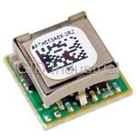
NON-ISOLATED DC/DC CONVERTERS 2.4-5.5VIN 3A 0.6-3.63VOUT
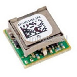
NON-ISOLATED DC/DC CONVERTERS SMT IN 2.4-5.5VDC OUT 0.59-3.63VDC 3A
22 W, 2.4 -5.5 VDC Vin, Single Output, 3.3 VDC@6.0 A Industrial DC-DC Converter
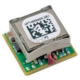
NON-ISOLATED DC/DC CONVERTERS SMT IN 2.4-5.5VDC OUT 0.59-3.63VDC 6A
Request a Quote

The quote request has been received
Close

Facing challenges or have inquiries? Feel free to contact us!
Call Us +1-469-283-2440
What they say about us
FANTASTIC RESOURCE
One of our top priorities is maintaining our business with precision, and we are constantly looking for affiliates that can help us achieve our goal. With the aid of GID Industrial, our obsolete product management has never been more efficient. They have been a great resource to our company, and have quickly become a go-to supplier on our list!
Bucher Emhart Glass
EXCELLENT SERVICE
With our strict fundamentals and high expectations, we were surprised when we came across GID Industrial and their competitive pricing. When we approached them with our issue, they were incredibly confident in being able to provide us with a seamless solution at the best price for us. GID Industrial quickly understood our needs and provided us with excellent service, as well as fully tested product to ensure what we received would be the right fit for our company.
Fuji
HARD TO FIND A BETTER PROVIDER
Our company provides services to aid in the manufacture of technological products, such as semiconductors and flat panel displays, and often searching for distributors of obsolete product we require can waste time and money. Finding GID Industrial proved to be a great asset to our company, with cost effective solutions and superior knowledge on all of their materials, it’d be hard to find a better provider of obsolete or hard to find products.
Applied Materials
CONSISTENTLY DELIVERS QUALITY SOLUTIONS
Over the years, the equipment used in our company becomes discontinued, but they’re still of great use to us and our customers. Once these products are no longer available through the manufacturer, finding a reliable, quick supplier is a necessity, and luckily for us, GID Industrial has provided the most trustworthy, quality solutions to our obsolete component needs.
Nidec Vamco
TERRIFIC RESOURCE
This company has been a terrific help to us (I work for Trican Well Service) in sourcing the Micron Ram Memory we needed for our Siemens computers. Great service! And great pricing! I know when the product is shipping and when it will arrive, all the way through the ordering process.
Trican Well Service
GO TO SOURCE
When I can't find an obsolete part, I first call GID and they'll come up with my parts every time. Great customer service and follow up as well. Scott emails me from time to time to touch base and see if we're having trouble finding something.....which is often with our 25 yr old equipment.
ConAgra Foods