

 Manufacturers
GE CRITICAL POWER QSDW035A0B641-PHZ
Description
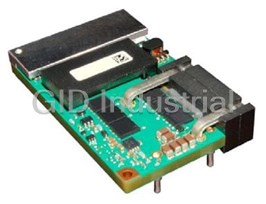
QSDW035A0B641-PHZ - BARRACUDA II
Part Number
QSDW035A0B641-PHZ
Price
Request Quote
Manufacturer
GE CRITICAL POWER
Lead Time
Request Quote
Category
Capacitors » DC-DC Converter
Specifications
Manufacturer
GE Critical Power
Manufacturers Part #
QSDW035A0B641-PHZ
Brand
GE Critical Power
Series
Barracuda
Factory Pack Quantity
24
Cooling Method
Convection
Dimensions
2.30 x 1.45 x 0.42"
Efficiency
95.5%
Industry
Industrial
Input Type
DC
Input Voltage Nominal
48 VDC
Isolation
2250 VDC
Mechanical Style
Isolated
Mounting
Through Hole
Number of Outputs
1
Operating Temperature
- 40 to + 85°C
Output Amps 1
35 A
Output Voltage V1 Nominal
12 VDC
Package Type
Enclosed
Subcategory
DC-DC Converter
Datasheet

Extracted Text
Data Sheet GE QSDW035A0B Barracuda Series* Power Modules; DC-DC Converters 36Vdc –75Vdc Input; 12Vdc Output; 35A Output Current Features Compliant to RoHS EU Directive 2011/65/EU (-Z versions) Compliant to REACH Directive (EC) No 1907/2006 Compatible with reflow pin/paste soldering process High efficiency – 95.5% at 12Vdc, 50% load to 100% load Wide Input voltage range: 36-75V dc Delivers up to 35A output current dc Output Voltage adjust: 5.0Vdc to 13.2Vdc Tightly regulated output voltage Low output ripple and noise Industry standard, DOSA compliant, Quarter brick: RoHS Compliant 58.4mm x 36.8 mm x 10.7 mm (2.30in x 1.45 in x 0.42 in) Applications Constant switching frequency Digital interface with PMBus™ Rev.1.2 compliance Distributed power architectures Positive Remote On/Off logic Intermediate bus voltage applications Output over current/voltage protection Servers and storage applications Over temperature protection Networking equipment including Power over Ethernet Wide operating temperature range (-40°C to 85°C) (PoE) † UL* 60950-1, 2nd Ed. Recognized, CSA C22.2 No. Fan assemblies other systems requiring a tightly ‡ 60950-1-07 Certified, and VDE (EN60950-1, 2nd regulated output voltage Ed.) Licensed § CE mark 2006/96/EC directives Options Meets the voltage and current requirements for ETSI 300- Negative Remote On/Off logic (1=option code, factory 132-2 and complies with and licensed for Basic insulation preferred) rating per EN60950-1 2250 Vdc Isolation tested in compliance with IEEE 802.3¤ PoE Auto-restart after fault shutdown (4=option code, standards factory preferred) ISO** 9001 and ISO14001 certified manufacturing facilities Base plate option (-H=option code) Passive Droop Load Sharing (-P=option code) Higher Output Capacitance (-Q=option code) Description The QSDW035A0B series of dc-dc converters are a new generation of DC/DC power modules designed to support 9.6 -12V dc intermediate bus applications where multiple low voltages are subsequently generated using point of load (POL) converters, as well as other application requiring a tightly regulated output voltage. The QSDW035A0B series operate from an input voltage range of 36 to 75Vdc, and provide up to 35A output current at output voltages from 5.0Vdc to 12.0Vdc. The 12V output is well regulated for the entire input voltage range. The QSDW035A0B has improved line transient performance as compared to earlier generation modules. The converter incorporates digital control, synchronous rectification technology, and innovative packaging techniques to achieve efficiency reaching 96% peak at 12Vdc output. This leads to lower power dissipation, such that, for many applications a heat sink is not required. Standard features include output voltage trim, remote sense, on/off control, output overcurrent and over voltage protection, over temperature protection, input under and over voltage lockout, power good signal and PMBus interface. The output is fully isolated from the input, allowing versatile polarity configurations and grounding connections. Built-in filtering for both input and output minimizes the need for external filtering. * Trademark of General Electric Company # UL is a registered trademark of Underwriters Laboratories, Inc. † CSA is a registered trademark of Canadian Standards Association. ‡ VDE is a trademark of Verband Deutscher Elektrotechniker e.V. § This product is intended for integration into end-user equipment . All of the required procedures of end-use equipment should be followed. ¤ IEEE and 802 are registered trademarks of the Institute of Electrical and Electronics Engineers, Incorporated. ** ISO is a registered trademark of the International Organization of Standards. June 1, 2016 ©2012 General Electric Company. All rights reserved. Page 1 Data Sheet GE QSDW035A0B Series Power Modules; DC-DC Converters 36Vdc –75Vdc Input; 12Vdc Output; 35A Output Current Absolute Maximum Ratings Stresses in excess of the absolute maximum ratings can cause permanent damage to the device. These are absolute stress ratings only, functional operation of the device is not implied at these or any other conditions in excess of those given in the operations sections of the Data Sheet. Exposure to absolute maximum ratings for extended periods can adversely affect device reliability. Parameter Device Symbol Min Max Unit Input Voltage* Continuous VIN -0.3 75 Vdc Operating transient ≤ 100mS 100 V dc Operating Input transient slew rate, 50V to 75V IN IN (Output may exceed regulation limits, no protective - - 5 V/µs shutdowns shall activate, C =220μF to C ) O O, max Non- operating continuous VIN 80 100 Vdc Operating Ambient Temperature All TA -40 85 °C (See Thermal Considerations section) Storage Temperature All T -55 125 °C stg I/O Isolation Voltage (100% factory Hi-Pot tested) All 2250 Vdc * Input over voltage protection will shut down the output voltage when the input voltage exceeds threshold level. Electrical Specifications Unless otherwise indicated, specifications apply over all operating input voltage, resistive load, and temperature conditions. Parameter Device Symbol Min Typ Max Unit Operating Input Voltage V 36 48 75 V IN dc Maximum Input Current IIN,max - - 13.5 Adc (V =0V to 75V, I =I ) IN O O, max Input No Load Current All I 87 mA IN,No load (VIN = VIN, nom, IO = 0, module enabled) Input Stand-by Current All I 30 mA IN,stand-by (VIN = VIN, nom, module disabled) External Input Capacitance All 100 - - μF 2 2 Inrush Transient All It - - 1 A s Input Terminal Ripple Current (Measured at module input pin with maximum specified input capacitance and ൏ 500uH inductance between All - 450 - mA rms voltage source and input capacitance C =220uF, 5Hz to IN 20MHz, VIN= 48V, IO= IOmax) Input Reflected Ripple Current, peak-to-peak (5Hz to 20MHz, 12μH source impedance; VIN= 48V, IO= All - 50 - mAp-p IOmax ; see Figure 11) Input Ripple Rejection (120Hz) All - 50 - dB CAUTION: This power module is not internally fused. An input line fuse must always be used. This power module can be used in a wide variety of applications, ranging from simple standalone operation to an integrated part of sophisticated power architecture. To preserve maximum flexibility, internal fusing is not included, however, to achieve maximum safety and system protection, always use an input line fuse. The safety agencies require a fast-acting fuse with a maximum rating of 25A (see Safety Considerations section). Based on the information provided in this Data Sheet on inrush energy and maximum dc input current, the same type of fuse with a lower rating can be used. Refer to the fuse manufacturer’s Data Sheet for further information. June 1, 2016 ©2012 General Electric Company. All rights reserved. Page 2 Data Sheet GE QSDW035A0B Series Power Modules; DC-DC Converters 36Vdc –75Vdc Input; 12Vdc Output; 35A Output Current Electrical Specifications (continued) Unless otherwise indicated, specifications apply over all operating input voltage, resistive load, and temperature conditions. Parameter Device Symbol Min Typ Max Unit Output Voltage Set-point (Default) All V 11.97 12.00 12.03 V O, set dc (VIN=VIN,nom, IO=17.5A, TA =25°C) (Adjustable via PMBus) Output Voltage All w/o -P VO 11.76 12.24 Vdc (Over all operating input voltage, resistive load, and -P Option VO 11.63 12.37 Vdc temperature conditions until end of life) Output Regulation Line All w/o -P 0.2 % V O, set Load All w/o -P 0.2 % VO, set Line -P Option 0.5 % VO, set Load, Intentional Droop -P Option 0.50 Vdc Temperature (T = -40ºC to +85ºC) All 2 % V A O, set Output Ripple and Noise on nominal output (V =V and I =I to I , tested with a 1.0 μF IN IN, nom O O, min O, max ceramic, 10 μF aluminum and 220μF polymer capacitor across the load.) RMS (5Hz to 20MHz bandwidth) All 70 mV rms Peak-to-Peak (5Hz to 20MHz bandwidth) All 200 mVpk-pk All except -Q 220 10,000 External Output Capacitance C μF O (For Co >5000µF, Io must be < 50% Io,max during Trise) -Q Option 6000 15,000 Output Current All Io 0 35 Adc VOUT_OC_FAULT_LIMIT (Default) (Adjustable via PMBus) All IO,lim 42 Adc Efficiency (VIN=VIN, nom, VO= VO,set, TA=25°C) IO= 100% IO, max All η 95.5 % IO= 55% - 90% IO, max All η 95.7 % Switching Frequency (primary MOSFETs) fsw 150 kHz (Output Ripple 2X switching frequency) Dynamic Load Response (dIo/dt=1A/10s; V =V ,nom; T =25°C; tested with a in in A 10 μF ceramic and 470μF polymer capacitor across the load.) Load Change from Io= 50% to 75% of Io,max: Vpk 750 mV Peak Deviation All pk ts __ 800 __ Settling Time (Vo<10% peak deviation) s Load Change from Io= 75% to 50% of Io,max: Peak Deviation Vpk __ 750 mVpk __ Settling Time (Vo<10% peak deviation) ts __ 800 s General Specifications Parameter Device Symbol Typ Unit Calculated Reliability Based upon Telcordia SR-332 Issue All MTBF 11,117,223 Hours 3: Method I, Case 3, (I =80%I , T =40°C, Airflow = 200 O O, max A 9 All FIT 90.0 10 /Hours LFM), 90% confidence Weight – Open Frame 49.6 (1.75) g (oz.) Weight – with Base plate option 69.2 (2.44) g (oz.) Isolation Specifications Parameter Symbol Min Typ Max Unit Isolation Capacitance C 2000 pF iso Isolation Resistance R 10 MΩ iso June 1, 2016 ©2012 General Electric Company. All rights reserved. Page 3 Data Sheet GE QSDW035A0B Series Power Modules; DC-DC Converters 36Vdc –75Vdc Input; 12Vdc Output; 35A Output Current Feature Specifications Unless otherwise indicated, specifications apply over all operating input voltage, resistive load, and temperature conditions. See Feature Descriptions for additional information. Parameter Device Symbol Min Typ Max Unit Remote On/Off Signal Interface (VIN=VIN, min to VIN, max , Signal referenced to VIN- terminal) Negative Logic: device code suffix “1” Logic Low = module On, Logic High = module Off Positive Logic: No device code suffix required Logic Low = module Off, Logic High = module On Logic Low Specification On/Off Thresholds: Remote On/Off Current – Logic Low All I 280 310 μA on/off Logic Low Voltage All Von/off -0.3 0.8 Vdc Logic High Voltage – (Typ = Open Collector) All V 2.0 14.5 V on/off dc Logic High maximum allowable leakage current All Ion/off 10 μA (Von/off = 2.0V) Maximum voltage allowed on On/Off pin All V 14.5 V on/off dc Turn-on Delay and Rise Time (I =I Adjustable via O O, max, PMBus) T delay, Enable with All w/o -P 150 ms Tdelay=Time until VO = 10% of VO,set from either Vin , application of Vin with Remote On/Off set to On Tdelay Enable with All w/o-P 10 ms (Enable with Vin); or operation of Remote On/Off from on/off Off to On with Vin already applied for at least 150 milli- Tdelay, Enable with w/ -P 180* ms seconds (Enable with on/off). Vin * Increased T due to startup for parallel modules. delay Tdelay, Enable with w/ -P 40* ms on/off T =Time for V to rise from 10% to 90% of V , For All w/o - rise O O,set T 25 ms rise C >5000uF, I must be < 50% I during T . P O O O, max rise * Increased Trise when Vo exists at startup for parallel w/ -P T 50* ms rise modules. Load Sharing Current Balance -P (difference in output current across all modules with I 3 A diff Option outputs in parallel, no load to full load) Remote Sense Range All VSense 0.5 Vdc Output Voltage Adjustment range (Adjustable via PMBus) All VO, set 5.0 13.2 Vdc Output Overvoltage Protection Setpoint (Adjustable via All V V +0.001V V +3.99V V O,OVPset O,SET O,SET dc PMBus) Output Voltage Peak Limits prior to OVP Protection, (100%-0% load dump, CO=COmin all VIN, IO) (5.0V ≤VO,SET≤12.0V) All VO,limit VO,OVPset-0.5V VO,OVPset +2.0V Vdc (12.01V ≤VO,SET≤13.2V) All VO,limit 15.49 17.99V Vdc Overtemperature Protection All Tref 135 °C (See Feature Descriptions) Input Undervoltage Lockout (Adjustable via PMBus) Turn-on Threshold 35 36 V dc Turn-off Threshold 31 33 V dc Input Overvoltage Lockout Turn-off Threshold 85 V dc Turn-on Threshold 80 Vdc Ω All 150 Pull down resistance of PGOOD pin Sink current capability into PGOOD pin (V =2.2V) PGAll 15 mA June 1, 2016 ©2012 General Electric Company. All rights reserved. Page 4 Data Sheet GE QSDW035A0B Series Power Modules; DC-DC Converters 36Vdc –75Vdc Input; 12Vdc Output; 35A Output Current Digital Interface Specifications Unless otherwise indicated, specifications apply over all operating input voltage, resistive load, and temperature conditions. See Feature Descriptions for additional information. Parameter Conditions Symbol Min Typ Max Unit PMBus Signal Interface Characteristics Input High Voltage (CLK, DATA) VIH 2.1 3.6 V Input Low Voltage (CLK, DATA) VIL 0.8 V Input high level current (CLK, DATA) I -10 10 μA IH Input low level current (CLK, DATA) IIL -10 10 μA Output Low Voltage (CLK, DATA, SMBALERT#) I=2mA VOL 0.4 V OUT Output high level open drain leakage current VOUT=3.6V IOH 0 10 μA (DATA, SMBALERT#) Pin capacitance CO 0.7 pF PMBus Operating frequency range (* 5-10 kHz to accommodate hosts not supporting Slave Mode FPMB 5* 400 kHz clock stretching) Measurement System Characteristics Output current reading range I 1.6500 63.937 A OUT(RNG) Output current reading blanking I 0 1.5875 A OUT(BNK) Output current reading resolution IOUT(RES) 62.5 mA Output current reading accuracy (Vin = 48V, 17.5A< Iout <35.0A I -6.0 6.0 % OUT(ACC) Vout =12V) Output current reading accuracy (absolute 1.75A< Iout <17.5A I -2 2 A OUT(ACC) difference between actual and reported values) VOUT reading range VOUT(RNG) 0 15.9997 V VOUT reading resolution VOUT(RES) 0.244 mV VOUT reading accuracy VOUT(ACC) -2.0 0.6 2.0 % V reading range V 0 127.875 V IN IN(RNG) V reading resolution V 125 mV IN IN(RES) V reading accuracy V -4.0 0.8 4.0 % IN IN(ACC) Temperature reading resolution T(RES) 0.25 °C Temperature reading accuracy T(ACC) -5.0 5.0 % June 1, 2016 ©2012 General Electric Company. All rights reserved. Page 5 Data Sheet GE QSDW035A0B Series Power Modules; DC-DC Converters 36Vdc –75Vdc Input; 12Vdc Output; 35A Output Current Characteristic Curves The following figures provide typical characteristics for the QSVW035A0B (12V, 35A) at 25ºC. The figures are identical for either positive or negative Remote On/Off logic. INPUT VOLTAGE, VO (V) OUTPUT CURRENT, IO (A) Figure 1. Typical Input Characteristic. Figure 2. Typical Converter Efficiency vs. Output Current. TIME, t (500 μs/div) TIME, t (2s/div) Figure 3. Typical Output Ripple and Noise, Io = Io,max, Co = Figure 4. Typical Transient Response to 0.1A/µs Step Co,min Change in Load from 50% to 75% to 50% of Full Load, Co=470µF and 48 Vdc Input. TIME, t (20 ms/div) TIME, t (10 ms/div) Figure 5. Typical Start-Up Using Vin with Remote On/Off Figure 6. Typical Start-Up Using Remote On/Off with Vin enabled, negative logic version shown. applied, negative logic version shown. June 1, 2016 ©2012 General Electric Company. All rights reserved. Page 6 OUTPUT VOLTAGE INPUT VOLTAGE OUTPUT VOLTAGE, INPUT CURRENT, Ii (A) V (V) (5V/div) V (V) (20V/div) O IN V (V) (50mV/div) O EFFCIENCY, η (%) OUTPUT CURRENT OUTPUT VOLTAGE OUTPUT VOLTAGE On/Off VOLTAGE I (A) (10A/div) V (V) (500mV/div) O O VO (V) (5V/div) VON/OFF (V)(2V/div) Data Sheet GE QSDW035A0B Series Power Modules; DC-DC Converters 36Vdc –75Vdc Input; 12Vdc Output; 35A Output Current Characteristic Curves (continued) INPUT VOLTAGE, Vin (V) OUTPUT CURRENT, IO (A) Figure 7. Typical Output Voltage Regulation vs. Input Figure 8. Typical Output Voltage Regulation vs. Output Voltage. Current. INPUT VOLTAGE, V (V) OUTPUT CURRENT, I (A) in O Figure 9. Typical Output Voltage Regulation vs. Input Figure 10. Typical Output Voltage Regulation vs. Output Voltage for the –P Version. Current for the –P Version. June 1, 2016 ©2012 General Electric Company. All rights reserved. Page 7 OUTPUT VOLTAGE, V (V) O OUTPUT VOLTAGE, V (V) O OUTPUT VOLTAGE, VO (V) OUTPUT VOLTAGE, VO (V) Data Sheet GE QSDW035A0B Series Power Modules; DC-DC Converters 36Vdc –75Vdc Input; 12Vdc Output; 35A Output Current Test Configurations Design Considerations Input Source Impedance The power module should be connected to a low ac-impedance source. A highly inductive source impedance can affect the stability of the power module. For the test configuration in Figure 11, a 220μF electrolytic capacitor, Cin, (ESR<0.7 at 100kHz), mounted close to the power module helps ensure the stability of the unit. If the module is subjected to rapid on/off cycles, a 330μF input capacitor is required. Consult the factory for further application guidelines. Note: Measure input reflected-ripple current with a simulated Safety Considerations source inductance (LTEST) of 12 µH. Capacitor CS offsets possible battery impedance. Measure current as shown above. For safety-agency approval of the system in which the power module is used, the power module must be installed Figure 11. Input Reflected Ripple Current Test Setup. in compliance with the spacing and separation requirements of the end-use safety agency standard, i.e., nd nd UL60950-1 2 Ed., CSA C22.2 No. 60950-1 2 Ed., and nd VDE0805-1 EN60950-1 2 Ed. If the input source is non-SELV (ELV or a hazardous voltage greater than 60 Vdc and less than or equal to 75Vdc), for the module’s output to be considered as meeting the requirements for safety extra-low voltage (SELV), all of the following must be true: The input source is to be provided with reinforced insulation from any other hazardous voltages, including the ac mains. One VIN pin and one VOUT pin are to be grounded, or Note: Use a 1.0 µF ceramic capacitor and a 10 µF aluminum or both the input and output pins are to be kept floating. tantalum capacitor. Scope measurement should be made The input pins of the module are not operator using a BNC socket. Position the load between accessible. 51 mm and 76 mm (2 in. and 3 in.) from the module. Another SELV reliability test is conducted on the whole Figure 12. Output Ripple and Noise Test Setup. system (combination of supply source and subject module), as required by the safety agencies, to verify CONTACT AND that under a single fault, hazardous voltages do not DISTRIBUTION LOSSES appear at the module’s output. VO1 VI(+) IO II Note: Do not ground either of the input pins of the module LOAD SUPPL Y without grounding one of the output pins. This may allow a non-SELV voltage to appear between the output pins and ground. VI(–) VO2 CONT ACT The power module has safety extra-low voltage (SELV) RESIST ANCE outputs when all inputs are SELV. Note: All measurements are taken at the module terminals. When The input to these units is to be provided with a maximum socketing, place Kelvin connections at module terminals to avoid 25A fast-acting (or time-delay) fuse in the ungrounded input measurement errors due to socket contact resistance. lead. The power module has internally generated voltages exceeding safety extra-low voltage. Consideration should be Figure 13. Output Voltage and Efficiency Test Setup. taken to restrict operator accessibility. June 1, 2016 ©2012 General Electric Company. All rights reserved. Page 8 Data Sheet GE QSDW035A0B Series Power Modules; DC-DC Converters 36Vdc –75Vdc Input; 12Vdc Output; 35A Output Current code suffix "1," is the factory-preferred configuration. The Feature Descriptions On/Off circuit is powered from an internal bias supply, Overcurrent Protection derived from the input voltage terminals. To turn the power module on and off, the user must supply a switch to control To provide protection in a fault output overload condition, the voltage between the On/Off terminal and the V (-) IN the module is equipped with internal current-limiting terminal (Von/off). The switch can be an open collector or circuitry and can endure current limiting continuously. If the equivalent (see Figure14). A logic LO is Von/off = -0.3V to 0.8V. overcurrent condition causes the output voltage to fall The typical Ion/off during a logic LO (Vin=48V, On/Off greater than 4.0V from Vo,set, the module will shut down and Terminal=0.3V) is 147µA. The switch should maintain a logic- remain latched off. The overcurrent latch is reset by either low voltage while sinking 310µA. During a logic HI, the cycling the input power or by toggling the on/off pin for one maximum Von/off generated by the power module is 8.2V. The second. If the output overload condition still exists when the maximum allowable leakage current of the switch at V = on/off module restarts, it will shut down again. This operation will 2.0V is 10µA. If using an external voltage source, the continue indefinitely until the overcurrent condition is maximum voltage V on the pin is 14.5V with respect to on/off corrected. the V (-) terminal. IN A factory configured auto-restart option (with overcurrent If not using the remote on/off feature, perform one of the and overvoltage auto-restart managed as a group) is also following to turn the unit on: available. An auto-restart feature continually attempts to For negative logic: short ON/OFF pin to V (-). restore the operation until fault condition is cleared. IN For positive logic: leave ON/OFF pin open. Output Overvoltage Protection The module contains circuitry to detect and respond to output overvoltage conditions. If the overvoltage condition causes the output voltage to rise above the limit in the Specifications Table, the module will shut down. The QSDW035A0B module is factory default configured for auto- restart operation. The auto-restart feature continually attempts to restore the operation until fault condition is cleared. If the output overvoltage condition still exists when the module restarts, it will shut down again. This operation will continue indefinitely until the overvoltage condition is corrected. Figure 14. Remote On/Off Implementation. A factory configured auto-restart option (with overcurrent and overvoltage auto-restart managed as a group) is also Load Sharing available. An auto-restart feature continually attempts to restore the operation until fault condition is cleared. For higher power requirements, the QSDW035A0 power module offers an optional feature for parallel operation (-P Overtemperature Protection Option code). This feature provides a precise forced output The modules feature an overtemperature protection circuit voltage load regulation droop characteristic. The output set to safeguard against thermal damage. The circuit shuts point and droop slope are factory calibrated to insure down the module when the default maximum device optimum matching of multiple modules’ load regulation reference temperature is exceeded. The module is factory characteristics. To implement load sharing, the following default configured to automatically restart once the requirements should be followed: reference temperature cools by ~25°C. The VOUT(+) and VOUT(-) pins of all parallel modules must be Input Under/Over Voltage Lockout connected together. Balance the trace resistance for each module’s path to the output power planes, to insure best At input voltages above or below the input under/over load sharing and operating temperature balance. voltage lockout limits, module operation is disabled. The VIN must remain between 36Vdc and 75Vdc for droop module will begin to operate when the input voltage level sharing to be functional. changes to within the under and overvoltage lockout limits. It is permissible to use a common Remote On/Off signal to start all modules in parallel. Remote On/Off These modules contain means to block reverse current The module contains a standard on/off control circuit flow upon start-up, when output voltage is present from reference to the V (-) terminal. Two factory configured IN other parallel modules, thus eliminating the requirement remote on/off logic options are available. Positive logic for external output ORing devices. Modules with the –P remote on/off turns the module on during a logic-high option will self-determine the presence of voltage on the voltage on the ON/OFF pin, and off during a logic LO. output from other operating modules, and automatically Negative logic remote on/off turns the module off during a increase its Turn On delay, Tdelay, as specified in the Feature logic HI, and on during a logic LO. Negative logic, device Specifications Table. June 1, 2016 ©2012 General Electric Company. All rights reserved. Page 9 Data Sheet GE QSDW035A0B Series Power Modules; DC-DC Converters 36Vdc –75Vdc Input; 12Vdc Output; 35A Output Current Feature Descriptions (continued) Pin Module Designation/Function Configuration When parallel modules startup into a pre-biased output, Code e.g. partially discharged output capacitance, the Trise is T/C1 C2 automatically increased, as specified in the Feature On/Off (O) Power Good w/o -P Factory Default Specifications table, to insure graceful startup. Trim On/Off (O) w/o -P Via PMBus Insure that the load is <50% IO,MAX (for a single module) Trim Power Good w/o -P Via PMBus until all parallel modules have started (load full start > On/Off (O) Power Good with -P Factory Default module T time max + T time). delay rise If fault tolerance is desired in parallel applications, output Remote On/Off(o) ORing devices should be used to prevent a single module The module contains an additional remote on/off control failure from collapsing the load bus. input On/Off(o), via either the T/C1 or C2 pin, reference to the Remote Sense V (-) terminal. The factory default configuration is set to O ignore this input, unless activated by the PMBus command, Remote sense minimizes the effects of distribution losses by MFR_ CPIN_ON_OFF_CONFIG. This command is also used to regulating the voltage at the remote-sense connections (See configure the logic for the On/Off(o) pin. Positive logic Figure 15). The SENSE(-) pin should be always connected to remote on/off turns the module on during a logic-high VO(–).The voltage between the remote-sense pins and the voltage on the ON/OFF pin, and off during a logic low. output terminals must not exceed the output voltage sense Negative logic remote on/off turns the module off during a range given in the Feature Specifications table: logic high, and on during a logic low. The On/Off(o) circuit is powered from an internal bias supply, referenced to [VO(+) – VO(–)] – [SENSE(+) ] 0.5 V SIG_GND. To turn the power module on and off, the user Although the output voltage can be increased by both the must supply a switch to control the voltage between the remote sense and by the trim, the maximum increase for On/Off (o) terminal and the V (-) terminal (V (o)). The O on/off the output voltage is not the sum of both. The maximum switch can be an open collector or equivalent (see Figure increase is the larger of either the remote sense or the trim. 13). A logic low is Von/off(o) = -0.3V to 0.8V. The typical Ion/off(o) The amount of power delivered by the module is defined as during a logic low is 330µA. The switch should maintain a the voltage at the output terminals multiplied by the output logic-low voltage while sinking 250µA. During a logic high, current. When using remote sense and trim, the output the maximum Von/off(o) generated by the power module is voltage of the module can be increased, which at the same 3.3V. The maximum allowable leakage current of the switch output current, would increase the power output of the at V (o) = 2.0V is 130µA. If using an external voltage on/off module. Care should be taken to ensure that the maximum source, the maximum voltage V on the pin is 3.3V with on/off output power of the module remains at or below the respect to the V (-) terminal. i maximum rated power (Maximum rated power = Vo,set x Io,max). If not using the Remote On/Off(o) feature, the pin may be left N/C. Power Good, PG The QSDW035A0B module provides a Power Good (PG) feature, which compares the module’s output voltage to the module’s POWER_GOOD_ON and POWER_GOOD_OFF values. These values are adjustable via PMBus. PG is asserted when the module’s output voltage is above the POWER_GOOD_ON value, and PG is de-asserted if any condition such as overtemperature, overcurrent or loss of Figure 15. Circuit Configuration for remote sense. regulation occurs that would result in the output voltage Configurable Control Pins going below the POWER_GOOD_OFF value. The QSDW035A0B contains two configurable control pins, The PG signal, provided on pin C2, is implemented with an T/C1 and C2, referenced to the module secondary SIG_GND. open-drain node, pulled up via a 10kΩ resistor to 3.3V See Mechanical Views for pin locations. The following table internally. For Positive Logic PG (default), the PG signal is HI, list the default factory configurations for the functions when PG is asserted, and LO, when the PG is de-asserted. assigned to these pins. Additional configurations can be For Negative Logic PG, the PG signal is LO, when PG is accomplished via the PMBus command, asserted, and HI, when the PG is de-asserted. MFR_CPIN_ARA_CONFIG. Following the table, there is a The PMBus command MFR_PGOOD _POLARITY is used to set feature description for each function. the logic polarity of the signal. If not using the Power Good feature, the pin may be left N/C. June 1, 2016 ©2012 General Electric Company. All rights reserved. Page 10 Data Sheet GE QSDW035A0B Series Power Modules; DC-DC Converters 36Vdc –75Vdc Input; 12Vdc Output; 35A Output Current Trim, Output Voltage Programming 5.11 12 .0 (100 5) 511 R 10 .22 trimup 1.225 5 5 Trimming allows the output voltage set point to be R 938.8 trimup increased or decreased; this is accomplished by connecting an external resistor between the TRIM pin and either the The voltage between the Vo(+) and Vo(–) terminals must not VO(+) pin or the VO(-) pin. exceed the minimum output overvoltage protection value shown in the Feature Specifications table. This limit includes any increase in voltage due to remote-sense compensation and output voltage set-point adjustment trim. Although the output voltage can be increased by both the remote sense and by the trim, the maximum increase for the output voltage is not the sum of both. The maximum increase is the larger of either the remote sense or the trim. The amount of power delivered by the module is defined as the voltage at the output terminals multiplied by the output current. When using remote sense and trim, the output voltage of the module can be increased, which at the same output current would increase the power output of the module. Care should be taken to ensure that the maximum output power of the module remains at or below the Figure 15. Circuit Configuration to Trim Output Voltage. maximum rated power (Maximum rated power = VO,set x Connecting an external resistor (R ) between the T/C1 trim-down IO,max). pin and the Vo(-) (or Sense(-)) pin decreases the output voltage set point. To maintain set point accuracy, the trim resistor tolerance should be ±1.0%. The following equation determines the required external resistor value to obtain a percentage output voltage change of ∆%. 511 R 10 .22 trimdown % Where 12 .0V V desired % 100 12 .0V For example, to trim-down the output voltage of the module by 20% to 9.6V, Rtrim-down is calculated as follows: % 20 511 R 10.22 trimdown 20 R 15.3k trimdown Connecting an external resistor (R ) between the T/C1 trim-up pin and the V (+) (or Sense (+)) pin increases the output O voltage set point. The following equations determine the required external resistor value to obtain a percentage output voltage change of ∆%: 5.11 12 .0V (100 %) 511 R 10 .22 trimup 1.225 % % V 12 .0V Where desired % 100 12 .0V For example, to trim-up the output voltage of the module by 5% to 12.6V, R is calculated as follows: trim-up % 5 June 1, 2016 ©2012 General Electric Company. All rights reserved. Page 11 Data Sheet GE QSDW035A0B Series Power Modules; DC-DC Converters 36Vdc –75Vdc Input; 12Vdc Output; 35A Output Current Feature Descriptions (continued) Thermal Considerations The thermal data presented here is based on physical measurements taken in a wind tunnel, using automated thermo-couple instrumentation to monitor key component temperatures: FETs, diodes, control ICs, magnetic cores, ceramic capacitors, opto-isolators, and module pwb conductors, while controlling the ambient airflow rate and temperature. For a given airflow and ambient temperature, . the module output power is increased, until one (or more) of Figure 16. Location of the thermal reference temperature the components reaches its maximum derated operating TH. temperature, as defined in IPC-9592B. This procedure is then repeated for a different airflow or ambient temperature until a family of module output derating curves is obtained. Figure 17. Location of the thermal reference temperature TH3 for Baseplate module. The output power of the module should not exceed the rated power for the module as listed in the Ordering Information table. Please refer to the Application Note “Thermal Characterization Process For Open-Frame Board-Mounted Power Modules” for a detailed discussion of thermal aspects The power modules operate in a variety of thermal including maximum device temperatures. environments and sufficient cooling should be provided to Heat Transfer via Convection help ensure reliable operation. Thermal considerations include ambient temperature, airflow, module power Increased airflow over the module enhances the heat dissipation, and the need for increased reliability. A transfer via convection. The thermal derating of figure 18- reduction in the operating temperature of the module will 19 shows the maximum output current that can be result in an increase in reliability. delivered by each module in the indicated orientation without exceeding the maximum THx temperature versus Heat-dissipating components are mounted on the top side local ambient temperature (TA) for several air flow of the module. Heat is removed by conduction, convection conditions. and radiation to the surrounding environment. Proper cooling can be verified by measuring the thermal reference The use of Figure 18 is shown in the following example: temperature (TH1 or TH2). Peak temperature occurs at the Example position indicated in Figure 16 and 17. For reliable operation What is the minimum airflow necessary for a QSDW035A0B this temperature should not exceed TREF = 125°C, and operating at VI = 48 V, an output current of 20A, and a TREF1=105°C or TREF2=105°C. For extremely high reliability maximum ambient temperature of 60 °C in transverse you can limit this temperature to a lower value. orientation. Solution: Given: V = 48V, I = 20A, T = 60 °C in O A Determine required airflow velocity (Use Figure 18): Velocity = 0.5m/s (100 LFM) or greater. June 1, 2016 ©2012 General Electric Company. All rights reserved. Page 12 Data Sheet GE QSDW035A0B Series Power Modules; DC-DC Converters 36Vdc –75Vdc Input; 12Vdc Output; 35A Output Current Thermal Considerations (continued) LOCAL AMBIENT TEMPERATURE, T (C) A Figure 20. Output Current Derating for the Base plate LOCAL AMBIENT TEMPERATURE, T (C) A QSDW035A0B-H with 0.25” heatsink in the Transverse Figure 18. Output Current Derating for the Open Frame Orientation; Airflow Direction from Vin(-) to Vin(+); Vin = QSDW035A0B in the Transverse Orientation; Airflow 48V Direction from Vin(-) to Vin(+); Vin = 48V. LOCAL AMBIENT TEMPERATURE, TA (C) LOCAL AMBIENT TEMPERATURE, TA (C) Figure 21. Output Current Derating for the Base plate Figure 19. Output Current Derating for the Base plate QSDW035A0B-H with 0.5” heatsink in the Transverse QSDW035A0B-H in the Transverse Orientation; Airflow Orientation; Airflow Direction from Vin(-) to Vin(+); Vin = Direction from Vin(-) to Vin(+); Vin = 48V. 48V LOCAL AMBIENT TEMPERATURE, T (C) A Figure 22. Output Current Derating for the Base plate QSDW035A0B-H with 1.0” heatsink in the Transverse Orientation; Airflow Direction from Vin(-) to Vin(+); Vin = 48V. June 1, 2016 ©2012 General Electric Company. All rights reserved. Page 13 OUTPUT CURRENT, IO (A) OUTPUT CURRENT, I (A) O OUTPUT CURRENT, IO (A) OUTPUT CURRENT, I (A) OUTPUT CURRENT, I (A) O O Data Sheet GE QSDW035A0B Series Power Modules; DC-DC Converters 36Vdc –75Vdc Input; 12Vdc Output; 35A Output Current linear reflow profile using Sn/Ag/Cu solder is shown in Figure Layout Considerations 23. The QSDW035A0B power module series are low profile in order to be used in fine pitch system card architectures. As such, component clearance between the bottom of the power module and the mounting board is limited. Avoid placing copper areas on the outer layer directly underneath the power module. Also avoid placing via interconnects underneath the power module. For additional layout guide-lines, refer to FLTR100V10 Data Sheet. Through-Hole Lead-Free Soldering Information The RoHS-compliant, Z version, through-hole products use the SAC (Sn/Ag/Cu) Pb-free solder and RoHS-compliant components. The non-Z version products use lead-tin Figure 23. Recommended linear reflow profile using (Pb/Sn) solder and RoHS-compliant components. Both Sn/Ag/Cu solder. version modules are designed to be processed through single or dual wave soldering machines. The pins have an RoHS-compliant, pure tin finish that is compatible with both MSL Rating Pb and Pb-free wave soldering processes. A maximum The QSDW035A0B modules have a MSL rating of 2a. preheat rate of 3C/s is suggested. The wave preheat process should be such that the temperature of the power Storage and Handling module board is kept below 210C. For Pb solder, the The recommended storage environment and handling recommended pot temperature is 260C, while the Pb-free procedures for moisture-sensitive surface mount packages solder pot is 270C max. Not all RoHS-compliant through- is detailed in J-STD-033 Rev. A (Handling, Packing, Shipping hole products can be processed with paste-through-hole Pb and Use of Moisture/Reflow Sensitive Surface Mount or Pb-free reflow process. If additional information is Devices). Moisture barrier bags (MBB) with desiccant are needed, please consult with your GE representative for more required for MSL ratings of 2 or greater. These sealed details. packages should not be broken until time of use. Once the original package is broken, the floor life of the product at Reflow Lead-Free Soldering Information conditions of 30°C and 60% relative humidity varies The RoHS-compliant through-hole products can be according to the MSL rating (see J-STD-033A). The shelf life processed with the following paste-through-hole Pb or Pb- for dry packed SMT packages will be a minimum of 12 free reflow process. months from the bag seal date, when stored at the following conditions: < 40° C, < 90% relative humidity. Max. sustain temperature : 245C (J-STD-020C Table 4-2: Packaging Thickness>=2.5mm Post Solder Cleaning and Drying 3 / Volume > 2000mm ), Considerations Peak temperature over 245C is not suggested due to the potential reliability risk of components under continuous Post solder cleaning is usually the final circuit-board high-temperature. assembly process prior to electrical board testing. The result Min. sustain duration above 217C : 90 seconds of inadequate cleaning and drying can affect both the Min. sustain duration above 180C : 150 seconds reliability of a power module and the testability of the Max. heat up rate: 3C/sec finished circuit-board assembly. For guidance on Max. cool down rate: 4C/sec appropriate soldering, cleaning and drying procedures, refer In compliance with JEDEC J-STD-020C spec for 2 times to GE Board Mounted Power Modules: Soldering and reflow requirement. Cleaning Application Note (AP01-056EPS). Pb-free Reflow Profile BMP module will comply with J-STD-020 Rev. C (Moisture/Reflow Sensitivity Classification for Nonhermetic Solid State Surface Mount Devices) for both Pb-free solder profiles and MSL classification procedures. BMP will comply with JEDEC J-STD-020C specification for 3 times reflow requirement. The suggested Pb-free solder paste is Sn/Ag/Cu (SAC). The recommended June 1, 2016 ©2012 General Electric Company. All rights reserved. Page 14 Data Sheet GE QSDW035A0B Series Power Modules; DC-DC Converters 36Vdc –75Vdc Input; 12Vdc Output; 35A Output Current cause for the SMBALERT. The CLEAR_FAULTS command will Digital Feature Descriptions retire the active SMBALERT. However, when the PMBus Interface Capability QSDW035A0B module is used in systems that do support ARA, Bit 4 of the MFR_CPIN_ARA_CONFIG command can be The QSDW035A0B series is equipped with a digital PMBus used to reconfigure the module to utilize ARA. In this case, interface to allow the module to be configured, and the QSDW035A0B will no longer respond to its programmed communicate with system controllers. Detailed timing and address, when in an ALERT active state. The master is electrical characteristics of the PMBus can be found in the expected to perform the modified received byte operation, PMB Power Management Protocol Specification, Part 1, and retire the ALERT active signal. At this time, the revision 1.2, available at http://pmbus.org. The QSDW035A0B will return to its resistor programmed QSDW035A0B supports both the 100kHz and 400kHz bus address, allowing normal master-slave communications to timing requirements. The QSDW035A0B shall stretch the proceed. The QSDW035A0B does not contain capability to clock, as long as it does not exceed the maximum clock LO arbitrate data bus contention caused by multiple modules period of 35ms. The QSDW035A0B will check the Packet responding to the modified received byte operation. Error Checking scheme (PEC) byte, if provided by the PMBus Therefore, when the ARA is used in a multiple module PMBus master, and include a PEC byte in all responses to the application, it is necessary to have the QSDW035A0B master. However, the QSDW035A0B does not require a PEC module at the lowest programmed address in order for the byte from the PMBus master. host to properly determine all modules’ address that are associated with an active SMBAlert. Please contact your GE The QSDW035A0B supports a subset of the commands in sales representative for further assistance, and for more the PMBus 1.2 specification. Most all of the controller information on the SMBus alert response protocol, see the parameters can be programmed using the PMBus and System Management Bus (SMBus) specification. stored as defaults for later use. All commands that require data input or output use the linear format. The exponent of PMBus Addressing the data words is fixed at a reasonable value for the The power module can be addressed through the PMBus command and altering the exponent is not supported. using a device address. The module has 64 possible Direct format data input or output is not supported by the addresses (0 to 63 in decimal) which can be set using QSDW035A0B. The supported commands are described in resistors connected from the ADDR0 and ADDR1 pins to greater detail below. GND. Note that some of these addresses (0 through 12, 40, 44, 45, and 55 in decimal) are reserved according to the The QSDW035A0B contains non-volatile memory that is SMBus specifications and may not be useable. The address used to store configuration settings and scale factors. The is set in the form of two octal (0 to 7) digits, with each pin settings programmed into the device are not automatically setting one digit. The ADDR1 pin sets the high order digit and saved into this non-volatile memory though. The ADDR0 sets the low order digit. The resistor values STORE_DEFAULT_ALL command must be used to commit suggested for each digit are shown in Table 4 (1% tolerance the current settings to non-volatile memory as device resistors are recommended). defaults. The settings that are capable of being stored in Table 4 non-volatile memory are noted in their detailed descriptions. Digit Resistor SMBALERT Interface Capability Value (KΩ) The QSDW035A0B also supports the SMBALERT response 0 10 protocol. The SMBALERT response protocol is a mechanism through which the QSDW035A0B can alert the PMBus 1 15.4 master that it has an active status or alarm condition via 2 23.7 pulling the SMBALERT pin to an active low. The master processes this condition, and simultaneously addresses all 3 36.5 slaves on the PMBus through the Alert Response Address. 4 54.9 Only the slave(s) that caused the alert (and that support the protocol) acknowledges this request. The master performs a 5 84.5 modified receive byte operation to get the slave’s address. 6 130 At this point, the master can use the PMBus status 7 200 commands to query the slave that caused the alert. Note: The QSDW035A0B can only respond to a single address at any given time. Therefore, the factory default state for the QSDW035A0B module is to retain its resistor programmed address, when it is in an ALERT active condition, and not respond to the ARA. This allows master systems, which do not support ARA, to continue to communicate with the slave QSDW035A0B using the programmed address, and using the various READ_STATUS commands to determine the June 1, 2016 ©2012 General Electric Company. All rights reserved. Page 15 Data Sheet GE QSDW035A0B Series Power Modules; DC-DC Converters 36Vdc –75Vdc Input; 12Vdc Output; 35A Output Current The module can also be turned on and off via the PMBus interface. The OPERATION command is used to actually turn ADDR1 the module on and off via the PMBus, while the ON_OFF_CONFIG command configures the combination of ADDR0 analog ON/OFF pin input and PMBus commands needed to turn the module on and off. Bit [7] in the OPERATION R R ADDR0 ADDR1 command data byte enables the module, with the following functions: SIG_GND 0 : Output is disabled 1 : Output is enabled Figure 24. Circuit showing connection of resistors used to set the PMBus address of the module. This module uses the lower five bits of the ON_OFF_CONFIG data byte to set various ON/OFF options as follows: 2 The user must know which I C addresses are reserved in a system for special functions and set the address of the Bit Position 4 3 2 1 0 module to avoid interfering with other system operations. Access r r/w r r r Both 100kHz and 400kHz bus speeds are supported by the Function PU CMD CPR POL CPA module. Connection for the PMBus interface should follow Default Value 1 1 1 1 1 the High Power DC specifications given in section 3.1.3 in the PU: Factory set to 1. QSDW035A0B requires On/Off(i) pin to SMBus specification V2.0 for the 400kHz bus speed or the be connected to proper input rail for module to power up. Low Power DC specifications in section 3.1.2. The complete This bit is used together with the CMD, CPR and ON bits to SMBus specification is available from the SMBus web site, determine startup. smbus.org. Bit Value Action PMBus Data Format Module does not power up until commanded by the analog ON/OFF pin and the OPERATION For commands that set or report any voltage thresholds 1 command as programmed in bits [2:0] of the related to output voltage (including VOUT_COMMAND, ON_OFF_CONFIG register. VOUT_MARGIN, POWER_GOOD and READ_VOUT), the module supports the linear data format consisting of a two byte value with a 16-bit, unsigned mantissa, and a fixed CMD: The CMD bit controls how the device responds to the exponent of -12. The format of the two data bytes is shown OPERATION command. below: Bit Value Action Module ignores the ON bit in the OPERATION 0 command Module responds to the ON bit in the 1 OPERATION command CPR: Factory set to 1. QSDW035A0B requires On/Off(i) pin to be connected to proper input rail for module to power up. The value of the number is then given by This bit is used together with the CMD and ON bits to -12 Value = Mantissa x 2 determine startup. For commands that set all other thresholds, voltages or Bit Value Action report such quantities, the module supports the linear data Module requires the analog ON/OFF pin to be 1 format consisting of a two byte value with an 11-bit, two’s asserted to start the unit complement mantissa and a 5-bit, two’s complement exponent. The format of the two data bytes is shown below: PMBus Adjustable Input Undervoltage Lockout The module allows adjustment of the input under voltage lockout and hysteresis. The command VIN_ON allows setting the input voltage turn on threshold, while the VIN_OFF command sets the input voltage turn off threshold. For both the VIN_ON and VIN_OFF commands, possible values range from 32.000 to 46.000V in 0.125V steps. VIN_ON must be 2.000V greater than VIN_OFF. The value is of the number is then given by Both the VIN_ON and VIN_OFF commands use the “Linear” format with two data bytes. The upper five bits [7:3] of the Exponent Value = Mantissa x 2 high data byte form the two’s complement representation of the exponent, which is fixed at –3 (decimal). The remaining PMBus Enabled On/Off June 1, 2016 ©2012 General Electric Company. All rights reserved. Page 16 Data Sheet GE QSDW035A0B Series Power Modules; DC-DC Converters 36Vdc –75Vdc Input; 12Vdc Output; 35A Output Current 11 bits are used for two’s complement representation of the 1010 : Margin High (Act on Fault) th mantissa, with the 11 bit fixed at zero since only positive Measuring Output Voltage Using the PMBus numbers are valid. The data associated with VIN_ON and VIN_OFF can be stored to non-volatile memory using the The module can provide output voltage information using STORE_DEFAULT_ALL command. the READ_VOUT command. The command returns two bytes of data in the linear format, with the 16 bits of the PMBus Adjustable Soft Start Delay and Rise Time READ_VOUT formatted as an unsigned mantissa, and a fixed The soft start delay and rise time can be adjusted in the exponent of -12 (decimal). module via PMBus. The TON_DELAY command sets the During module manufacture, an offset correction value is delay time in ms, and allows choosing delay times between written into the non-volatile memory of the module to null 10ms and 500ms, with resolution of 0.5ms. The TON_RISE errors in the tolerance and A/D conversion of VOUT. The command sets the rise time in ms, and allows choosing soft command MFR_VOUT_READ_CAL_OFFSET can be used to start times between 15ms and 500ms, with resolution of read the offset - two bytes consisting of a signed 16-bit 0.5ms. When setting TON_RISE, make sure that the charging mantissa in two’s complement format, using a fixed current for output capacitors can be delivered by the exponent of -12 (decimal). The resolution is 0.244mV. The module in addition to any load current to avoid nuisance corrected Output voltage reading is then given by: tripping of the overcurrent protection circuitry during startup. Both the TON_RISE and TON_DELAY commands use V (Read)[V (A/D) the “Linear” format with two data bytes. The upper five bits OUT OUT [7:3] of the high data byte form the two’s complement MFR_VOUT_READ_CAL_OFFSET representation of the exponent, which is fixed at –1 (decimal). The remaining 11 bits are used for two’s Measuring Input Voltage Using the PMBus th complement representation of the mantissa, with the 11 bit fixed at zero since only positive numbers are valid. The The module can provide input voltage information using the data associated with TON_RISE and TON_DELAY can be READ_VIN command. The command returns two bytes of stored to non-volatile memory using the data in the linear format. The upper five bits [7:3] of the high data byte form the two’s complement representation of the STORE_DEFAULT_ALL command. exponent, which is fixed at –3 (decimal). The remaining 11 Output Voltage Adjustment Using the PMBus bits are used for two’s complement representation of the th mantissa, with the 11 bit fixed at zero since only positive The QSDW035A0B module output voltage set point is numbers are valid. adjusted using the VOUT_COMMAND. The output voltage setting uses the Linear data format, with the 16 bits of the During module manufacture, offset and gain correction VOUT_COMMAND formatted as an unsigned mantissa, and values are written into the non-volatile memory of the a fixed exponent of -12 (decimal) (read from VOUT_MODE). module to null errors in the tolerance and A/D conversion of -12 Vin. The command MFR_VIN_READ_CAL_OFFSET can be VOUT = Mantissa x 2 used to read the offset - two bytes consisting of a five-bit The range limits for VOUT_COMMAND are 8.10V to 13.20V, exponent (fixed at -3) and a 11-bit mantissa in two’s and the resolution is 0.244mV. complement format. The resolution is 125mV. The command The data associated with VOUT_COMMAND can be stored to MFR_VIN_READ_CAL_GAIN can be used to read the gain non-volatile memory using the STORE_DEFAULT_ALL correction - two bytes consisting of a unsigned 16 bit command. number. The resolution of this correction factor 0.000122. The corrected input voltage reading is then given by: Output Voltage Margining Using the PMBus The QSDW035A0B module can also have its output voltage V (Read) IN margined via PMBus commands. The command [V (A/D)(MFR_VIN_READ _CAL_GAIN/8192 )] IN VOUT_MARGIN_HIGH sets the margin high voltage, while the command VOUT_MARGIN_LOW sets the margin low voltage. MFR_VIN_READ _CAL_OFFSET Both the VOUT_MARGIN_HIGH and VOUT_MARGIN_LOW commands use the “Linear” mode with the exponent fixed at Measuring Output Current Using the PMBus –12 (decimal). The data associated with The module measures output current by using the output VOUT_MARGIN_HIGH and VOUT_MARGIN_LOW can be filter inductor winding resistance as a current sense stored to non-volatile memory using the element. The module can provide output current STORE_DEFAULT_ALL command. information using the READ_IOUT command. The command The module is commanded to go to the margined high or returns two bytes of data in the linear format. The upper five low voltages using the OPERATION command. Bits [5:2] are bits [7:3] of the high data byte form the two’s complement used to enable margining as follows: representation of the exponent, which is fixed at –4 (decimal). The remaining 11 bits are used for two’s 00XX : Margin Off th complement representation of the mantissa, with the 11 0110 : Margin Low (Act on Fault) June 1, 2016 ©2012 General Electric Company. All rights reserved. Page 17 Data Sheet GE QSDW035A0B Series Power Modules; DC-DC Converters 36Vdc –75Vdc Input; 12Vdc Output; 35A Output Current bit fixed at zero since only positive numbers are valid. STATUS_WORD : Returns two bytes of information with a Output current readings are blanked below 1.65A. summary of the module’s fault/warning conditions. High Byte During module manufacture, offset and gain correction Bit Position Flag Default Value values are written into the non-volatile memory of the 15 VOUT fault 0 module to null errors in the tolerance and A/D conversion of 14 IOUT fault or warning 0 IOUT. The command MFR_IOUT_CAL_OFFSET can be used to 13 Input Voltage fault 0 read the offset - two bytes consisting of a five-bit exponent 12 X 0 (fixed at -4) and a 11-bit mantissa in two’s complement 11 POWER_GOOD# (is negated) 0 format. The resolution is 62.5mA. The command 10 X 0 MFR_IOUT_CAL_GAIN can be used to read the gain 9 X 0 correction - two bytes consisting of a unsigned 16 bit 8 X 0 number. The resolution of this correction factor 0.000122. Low Byte The READ_IOUT command provides module average output Bit Position Flag Default Value current information. This command only supports positive 7 X 0 current sourced from the module. If the converter is sinking 6 OFF 0 current a reading of 0 is provided. 5 VOUT Overvoltage 0 I (Read) OUT 4 IOUT Overcurrent 0 3 VIN Undervoltage 0 [I (A/D)(MFR_IOUT _CAL_GAIN/8192)] OUT 2 Temperature 0 MFR_IOUT _CAL_OFFSET 1 CML (Comm. Memory Fault) 0 Note that the current reading provided by the module is 0X 0 corrected for temperature. STATUS_VOUT : Returns one byte of information relating to Measuring the Temperature using the PMBus the status of the module’s output voltage related faults. Bit Position Flag Default Value The module can provide temperature information using the READ_TEMPERATURE_1 command. The command returns 7 VOUT OV Fault 0 two bytes of data in the linear format. The upper five bits 6 X 0 [7:3] of the high data byte form the two’s complement 5 X 0 representation of the exponent, which is fixed at –2 4 X 0 (decimal). The remaining 11 bits are used for two’s 3 X 0 complement representation of the mantissa. 2 X 0 1 X 0 Note that the module’s temperature sensor is located close 0 X 0 to the module hot spot TH (see Thermal Considerations).and 1 is subjected to temperatures higher than the ambient STATUS_IOUT : Returns one byte of information relating to air temperature near the module. The temperature reading the status of the module’s output currentrelated faults. will be highly influenced by module load and airflow Default conditions. Bit Position Flag Value Reading the Status of the Module using the PMBus 7 IOUT OC Fault 0 6X 0 The module supports a number of status information 5 IOUT OC Warning 0 commands implemented in PMBus. However, not all 4 X 0 features are supported in these commands. A X in the FLAG 3 X 0 cell indicates the bit is not supported. 2 X 0 1 X 0 0 X 0 June 1, 2016 ©2012 General Electric Company. All rights reserved. Page 18 Data Sheet GE QSDW035A0B Series Power Modules; DC-DC Converters 36Vdc –75Vdc Input; 12Vdc Output; 35A Output Current STATUS_INPUT : Returns one byte of information relating to the status of the module’s input voltage related faults. Bit Position Flag Default Value 7 VIN OV Fault 0 6 X 0 5 X 0 4 VIN UV Fault 0 3 Module Off (Low VIN) 0 2 X 0 1 X 0 0 X 0 STATUS_TEMPERATURE : Returns one byte of information relating to the status of the module’s temperature related faults. Bit Position Flag Default Value 7 OT Fault 0 6 OT Warning 0 5 X 0 4 X 0 3 X 0 2 X 0 1 X 0 0 X 0 STATUS_CML : Returns one byte of information relating to the status of the module’s communication related faults. Bit Position Flag Default Value Invalid/Unsupported 7 0 Command 6 Invalid/Unsupported Data 0 5 Packet Error Check Failed 0 4 X 0 3 X 0 2 X 0 1 X 0 0 X 0 June 1, 2016 ©2012 General Electric Company. All rights reserved. Page 19 Data Sheet GE QSDW035A0B Series Power Modules; DC-DC Converters 36Vdc –75Vdc Input; 12Vdc Output; 35A Output Current Summary of Supported PMBus Commands This section outlines the PMBus command support for the QSDW035A0B bus converters. Each supported command is outlined in order of increasing command codes with a quick reference table of all supported commands included at the end of the section. Each command will have the following basic information. Command Name [Code] Command support Data format Factory default Additional information may be provided in tabular form or other format, if necessary. OPERATION [0x01] Command support: On/Off Immediate and Margins (Act on Fault). Soft off with sequencing not supported and Margins (Ignore Fault) not supported. Therefore bits 6, 3, 2, 1 and 0 set as read only at factory defaults. Format 8 bit unsigned (bit field) Bit Position 7 6 5 4 3 2 1 0 Access r/w r r/w r/w r r r r Function ON/OFF Bits[5:4] Bits[3:2] N/A Default Value 1 0 0 0 1 0 0 0 ON_OFF_CONFIG [0x02] Command support: Bit 1 polarity will be set based upon module code [0=Negative on/off logic, 1=positive on/off logic to allow customer system to know hardware on/off logic Format 8 bit unsigned (bit field) Bit Position 7 6 5 4 3 2 1 0 Access r r r r r r/w r r Function (reserved) Bit 4 pu Bit 3 cmd Bit 2 cpr Bit 1 pol Bit 0 cpa module Default Value 0 0 0 1 1 1 1 code CLEAR_FAULTS [0x03] Command support: All functionality STORE_DEFAULT_ALL[0x11] Command support: All functionality – Stores operating parameters to EEprom memory. Command requires ≤ 500ms to execute. Delay any additional commands to module for sufficient time to complete execution. RESTORE_DEFAULT_ALL[0x12] Command support: All functionality – Restores operating parameters from EEprom memory. Command requires ≤ 200ms to execute. Delay any additional commands to module for sufficient time to complete execution. VOUT_MODE[0x20] Command support: Supported. Factory default: 0x14 – indicates linear mode with exp = -12 Format 8 bit unsigned (bit field) Bit Position 7 6 5 4 3 2 1 0 Access r r r r r r r r Function Mode (linear) 2’s complement exponent Default Value 0 0 0 1 0 1 0 0 VOUT_COMMAND [0x21] Data format: 16 bit unsigned mantissa (implied exponent per VOUT_MODE) -12 Factory default: 12.000V ( 12.00/2 → 49,152 = 0xC000 ) [standard code] Range limits (max/min): 13.200V/5.000V Units: volt Command support: Supported VOUT_CAL_OFFSET [0x23] Range limits (max/min): +0.25/-0.25 Units: volt Command support: read/write support, lockout per MFR_DEVICE_TYPE, functionality implemented June 1, 2016 ©2012 General Electric Company. All rights reserved. Page 20 Data Sheet GE QSDW035A0B Series Power Modules; DC-DC Converters 36Vdc –75Vdc Input; 12Vdc Output; 35A Output Current VOUT_MARGIN_HIGH [0x25] Range limits (max/min): 13.2/5.0 Units: volt Command support: read/write support, full functionality except “Ignore faults”. Note: Range cross-check - value must be greater than VOUT_MARGIN_LOW value. VOUT_MARGIN_LOW [0x26] Range limits (max/min): 13.2/5.0 Units: volt Command support: read/write support, full functionality except “Ignore faults”. Note: Range cross-check - value must be less than VOUT_MARGIN_HIGH value. VOUT_DROOP [0x28] Factory default: 0 (No droop); 14.3 (Parallel operation) Range limits (max/min): 50/0 Units: mv/A Command support: All functionality VIN_ON [0x35] Range limits (max/min): 46/33 Units: volt Command support: All functionality Note: Special interlock checks between VIN_ON and VIN_OFF maintain a hysteresis gap of 2V minimum and do not allow the OFF level to be higher than and ON level VIN_OFF [0x36] Range limits (max/min): 46/33 Units: volt Command support: All functionality Note: Special interlock checks between VIN_ON and VIN_OFF maintain a hysteresis gap of 2V minimum and do not allow the OFF level to be higher than and ON level VOUT_OV_FAULT_LIMIT [0x40] Range limits (max/min): 15.99/10.90 (See note 1, 2) Units: volt Command support: All functionality Note: 1. Range cross- check – value must be greater than VOUT_COMMAND value. 2. The module’s internal maximum OV Fault Limit equals the VOUT_COMMAND plus 3.99V, up to 15.99V. This is an automatic module protection feature that will override a user-set VOUT_OV_FAULT_LIMIT, if the user limit is set too high. The internal OV Fault limit value is not visible to the user via PMBus. VOUT_OV_FAULT_RESPONSE [0x41] Command support: ‐ Response settings (bits RSP0:1) – only a setting of 10, unit shuts down and responds according to the retry settings below, is supported. ‐ Retry settings (bits RS0:2) – only settings of 000 (unit does not attempt to restart on fault) and 111 unit continuously restarts (normal startup) while fault is present until commanded off, bias power is removed or another fault condition causes the unit to shutdown. ‐ Delay time setting (bits 0-2) – only DT0:2 = 0 (no delay) supported. Default Settings: The default settings for the VOUT_OV_FAULT_RESPONSE command are; ‐ The unit shuts down in response to a VOUT over voltage condition. ‐ The unit will continuously restart (normal startup) while the VOUT over voltage condition is present until it is commanded off, bias power is removed or another fault condition causes the unit to shutdown. ‐ The shutdown delay is set to 0 delay cycles. Format 8 bit unsigned (bit field) Bit Position 7 6 5 4 3 2 1 0 Access r r r/w r/w r/w r r r Function RSP[1] RSP[0] RS[2] RS[1] RS[0] DT[2] DT[1] DT[0] Default Value 1 0 1 1 1 0 0 0 June 1, 2016 ©2012 General Electric Company. All rights reserved. Page 21 Data Sheet GE QSDW035A0B Series Power Modules; DC-DC Converters 36Vdc –75Vdc Input; 12Vdc Output; 35A Output Current IOUT_OC_FAULT_LIMIT [0x46] Range limits (max/min): 50/15 Units: amp Command support: All functionality Note: Range cross-check – value must be greater than IOUT_OC_WARN_LIMIT value. IOUT_OC_FAULT_RESPONSE [0x47] Command support: ‐ Response settings (bits RSP0:1) – only settings of 11, unit shuts down and responds according to the retry settings below, is supported. ‐ Retry settings (bits RS0:2) – only settings of 000 (unit does not attempt to restart on fault) and 111 unit continuously restarts (normal startup) while fault is present until commanded off, bias power is removed or another fault condition causes the unit to shutdown. ‐ Delay time setting (bits 0-2) – only DT0:2 = 0 (no delay) supported. Default Settings: The default settings for the IOUT_OC_FAULT_RESPONSE command are; ‐ The unit shuts down in response to an IOUT over current condition. ‐ The unit will continuously restart (normal startup) while the IOUT over current condition is present until it is commanded off, bias power is removed or another fault condition causes the unit to shutdown. ‐ The shutdown delay is set to 0 delay cycles. Format 8 bit unsigned (bit field) Bit Position 7 6 5 4 3 2 1 0 Access r r r/w r/w r/w r r r Function RSP[1] RSP[0] RS[2] RS[1] RS[0] DT[2] DT[1] DT[0] Default Value 1 1 1 1 1 0 0 0 IOUT_OC_WARN_LIMIT [0x4A] Range limits (max/min): 40/8 Units: amp Command support: read/write support, functionality complete Note: Range cross-check – value must be less than IOUT_OC_FAULT_LIMIT value. OT_FAULT_LIMIT [0x4F] Range limits (max/min): 140/25 Units: degrees C. Command support: All functionality Note: Range cross-check – value must be greater than OT_WARN_LIMIT value. OT_FAULT_RESPONSE [0x50] Command support: ‐ Response settings (bits RSP0:1) – only setting of 10, unit shuts down and responds according to the retry settings below. ‐ Retry settings (bits RS0:2) – only settings of 000 (unit does not attempt to restart on fault) and 111 unit continuously restarts (normal startup) while fault is present until commanded off, bias power is removed or another fault condition causes the unit to shutdown. ‐ Delay time setting (bits 0-2) – only DT0:2 = 0 (no delay) supported. Default Settings: The default settings for the OT_FAULT_RESPONSE command are; ‐ The unit shuts down in response to an over-temperature condition. ‐ The unit will continuously restart (normal startup) while the over-temperature condition is present until it is commanded off, bias power is removed or another fault condition causes the unit to shutdown. ‐ The shutdown delay is set to 0 delay cycles. Format 8 bit unsigned (bit field) Bit Position 7 6 5 4 3 2 1 0 Access r r r/w r/w r/w r r r Function RSP[1] RSP[0] RS[2] RS[1] RS[0] DT[2] DT[1] DT[0] Default Value 1 0 1 1 1 0 0 0 June 1, 2016 ©2012 General Electric Company. All rights reserved. Page 22 Data Sheet GE QSDW035A0B Series Power Modules; DC-DC Converters 36Vdc –75Vdc Input; 12Vdc Output; 35A Output Current OT_WARN_LIMIT [0x51] Range limits (max/min): 125/25 Units: degrees C. Command support: All functionality Note: Range cross-check – value must be less than OT_FAULT_LIMIT value. VIN_OV_FAULT_LIMIT [0x55] Range limits (max/min): 90/48 Units: volt Command support: All functionality VIN_OV_FAULT_RESPONSE [0x56] Command support: Response settings (bits RSP0:1) – only settings of 11 (The device’s output is disabled while the fault is present.) is supported.. ‐ Retry settings (bits RS0:2) – only settings of 000 (unit does not attempt to restart on fault. ‐ Delay time setting (bits 0-2) – only DT0:2 = 0 (no delay) supported. Default Settings: The default settings for the VIN_OV_FAULT_RESPONSE command are; ‐ The unit shuts down in response to a VIN over voltage condition. ‐ The unit will continuously prepares to restart (normal startup) while the VIN over voltage condition is present until it is commanded off, bias power is removed, the VIN over voltage condition is removed, or another fault condition causes the unit to shutdown. ‐ The shutdown delay is set to 0 delay cycles. Format 8 bit unsigned (bit field) Bit Position 7 6 5 4 3 2 1 0 Access r r r r r r r r Function RSP[1] RSP[0] RS[2] RS[1] RS[0] DT[2] DT[1] DT[0] Default Value 1 1 0 0 0 0 0 0 POWER_GOOD_ON [0x5E] Range limits (max/min): 13.2/3.0 Units: volt Command support: full support Note: Range cross-check – value must be greater than POWER_GOOD_OFF value by 0.5V. POWER_GOOD_OFF [0x5F] Range limits (max/min): 13.2/3.0 Units: volt Command support: full support Note: Range cross-check – value must be less than POWER_GOOD_ON value by 0.5V. TON_DELAY [0x60] Range limits (max/min): 500/0 Units: milliseconds Command support: full support TON_RISE [0x61] Range limits (max/min): 500/15 Units: milliseconds Command support: full support STATUS_WORD [0x79] Command support: full implementation for supported functions (note: Fans, MFR_SPECIFIC, Unknown not supported) Format 8 bit unsigned (bit field) Bit Position 15 14 13 12 11 10 9 8 Access r r r r r r r r #PWR_ UN 1 1 1 Function VOUT I/POUT INPUT MFR_SPEC FANS OTHER 1 GOOD KNOWN Format 8 bit unsigned (bit field) Bit Position 7 6 5 4 3 2 1 0 June 1, 2016 ©2012 General Electric Company. All rights reserved. Page 23 Data Sheet GE QSDW035A0B Series Power Modules; DC-DC Converters 36Vdc –75Vdc Input; 12Vdc Output; 35A Output Current Access r r r r r r r r OUTPUT VOUT_O VIN_UV NONE OF 1 Function BUSY IOUT_OC _FAULT TEMP CML 1 _OFF V _FAULT _FAULT ABOVE (1) Not supported STATUS_VOUT [0x7A] Command support: VOUT_OV_FAULT support, all bit reset supported Format 8 bit unsigned (bit field) Bit Position 7 6 5 4 3 2 1 0 Access r/reset(1) r/ reset r/ reset r/ reset r/ reset r/ reset r/ reset r/ reset VOUT_ TON_ TOFF_ VOUT VOUT_OV VOUT_OV VOUT_UV VOUT_UV Function MAX_ MAX_ TRACKING MAX 1 1 1 _FAULT _WARN _WARN _FAULT 1 1 1 1 _WARN FAULT WARN ERROR (1) Not supported STATUS_IOUT [0x7B] Command support: IOUT_OC_FAULT support, all bit reset supported Format 8 bit unsigned (bit field) Bit Position 7 6 5 4 3 2 1 0 Access r/ reset(1) r/ reset r/ reset r/ reset r/ reset r/ reset r/ reset r/ reset Function In Power IOUT_OC IOUT_OC _LV IOUT_OC IOUT_UC Current Share POUT_OP POUT_OP Limiting 1 1 1 1 1 _FAULT _FAULT _WARN _FAULT Fault _FAULT _WARN 1 Mode (1) Not supported STATUS_INPUT [0x7C] Command support: VIN_OV_FAULT support, all bit reset supported Format 8 bit unsigned (bit field) Bit Position 7 6 5 4 3 2 1 0 Access r/ reset(1) r/ reset r/ reset r/ reset r/ reset r/ reset r/ reset r/ reset Unit Off VIN_OV VIN_OV VIN_UV VIN_UV IIN_OC IIN_OC PIN_OP Function (low input 1 1 1 1 1 _FAULT _WARN _WARN _FAULT _FAULT _WARN _WARN voltage) (1) Not supported STATUS_TEMPERATURE [0x7D] Command support: OT_WARN, OT_FAULT supported, all bit reset supported Format 8 bit unsigned (bit field) Bit Position 7 6 5 4 3 2 1 0 Access r/ reset(1) r/ reset r/ reset r/ reset r/ reset r/ reset r/ reset r/ reset UT_ UT_ Function OT_ FAULT OT_ WARN reserved reserved reserved reserved 1 1 WARN FAULT (1) Not supported June 1, 2016 ©2012 General Electric Company. All rights reserved. Page 24 Data Sheet GE QSDW035A0B Series Power Modules; DC-DC Converters 36Vdc –75Vdc Input; 12Vdc Output; 35A Output Current STATUS_CML [0x7E] Command support: PEC_FAULT, INVALID_DATA, INVALID_CMD supported, all bit reset supported Format 8 bit unsigned (bit field) Bit Position 7 6 5 4 3 2 1 0 Access r/ reset(1) r/ reset r/ reset r/ reset r/ reset r/ reset r/ reset r/ reset COM Memory/ INVALID INVALID MEMORY PROC Function PEC FAILED reserved FAULT Logic fault 1 1 CMD DATA FAULT FAULT 1 1 (other) (other) (1) Not supported READ_VIN [0x88] Command support: full support READ_VOUT [0x8B] Command support: full support READ_IOUT [0x8C] Command support: full support READ_TEMPERATURE_1 [0x8D] Command support: full support MFR_DEVICE_TYPE [0xD0] Command support: partial support in place (Mod Name) Format Unsigned Binary Bit Pos. 7 6 5 4 3 2 1 0 7 6 5 4 3 2 1 0 Access r/w r/w r/w r/w r/w r r r r/w r/w r/w r/w r/w r/w r/w r/w Function Reserved Module Name WPE Res Default 0 0 0 0 0 0 0 0 1 0 0 0 0 0 1 0 Byte Bit Description Value Meaning High Byte 7:0 Reserved 1 7:2 Module Name 1xxxxx Module Name 0 Write Protect Enable not active. Low Byte 1 WPE 1 Write Protect Enable active. 0 Reserved 0 Reserved 1. Present module designations (Non-isolated units will have a 0XXXXX format) QSDW035A0B4xxx: 100110 MFR_VOUT_READ_CAL_GAIN [0xD1] Factory default: 0x2000 Range limits (max/min): 0x2666/0x1999 Units: N/A Command support: support for VOUT gain calibration (factor in flash), lockout per MFR_DEVICE_TYPE MFR_VOUT_READ_CAL_OFFSET [0xD2] Range limits (max/min): exp must = -12 Units: N/A Command support: support for VOUT offset calibration (factor in flash), lockout per MFR_DEVICE_TYPE MFR_VIN_READ_CAL_GAIN [0xD3] Factory default: 0X2000 Range limits (max/min): 0x2666/0x1999 Command support: support for VIN gain calibration (factor in flash), lockout per MFR_DEVICE_TYPE June 1, 2016 ©2012 General Electric Company. All rights reserved. Page 25 Data Sheet GE QSDW035A0B Series Power Modules; DC-DC Converters 36Vdc –75Vdc Input; 12Vdc Output; 35A Output Current MFR_VIN_READ_CAL_OFFSET [0xD4] Data format: VIN linear format Range limits (max/min): exp must = -3 Units: N/A Command support: support for VIN offset calibration (factor in flash), lockout per MFR_DEVICE_TYPE MFR_IOUT_CAL_GAIN [0xD6] Range limits (max/min): 0x2666/0x1999 Units: N/A Command support: support for IOUT gain calibration, lockout per MFR_DEVICE_TYPE MFR_IOUT_CAL_OFFSET [0xD7] Range limits (max/min): exp must = -4 Units: N/A Command support: support for IOUT offset calibration, lockout per MFR_DEVICE_TYPE MFR_FW_REV [0xDB] Range limits (max/min): 0 - 0xff (0.00 – 15.15) Units: N/A Command support: full read support MFR_C1_C2_ARA_CONFIG [0xE0] Command Code Command support: Full support. The module must be configured with ENABLE_OFF when C1/C2 is being reconfigured. Command MFR_C1_C2_ARA_CONFIG Format 8 bit unsigned (bit field) Bit Position 7 6 5 4 3 2 1 0 Access r r r r/w r/w r/w r/w r/w Function Reserved ARA Assignment Table Default Value 0 0 0 0 0 0 0 0 Bit Description Value Meaning 7:5 Reserved 000 Reserved ARA not functional, module remains at resistor programmed address when SMBLAERT 0 is asserted 4 ARA 1 ARA functional, module responds to ARA only, when SMBLAERT is asserted T/C1 pin: ON/OFF (Secondary) 0000 C2 pin: POWER_GOOD PIN T/C1 pin: TRIM 3:0 0001 Configuration* C2 pin: POWER_GOOD T/C1 pin: TRIM 0010 C2 pin: ON/OFF (Secondary) * All QBDW without –P option Bit Description Value Meaning 7:5 Reserved 000 Reserved ARA not functional, module remains at resistor programmed address when SMBLAERT 0 is asserted 4 ARA 1 ARA functional, module responds to ARA only, when SMBLAERT is asserted PIN T/C1 pin: ON/OFF (Secondary) 3:0 0000 Configuration** C2 pin: POWER_GOOD ** All QBDW with –P option June 1, 2016 ©2012 General Electric Company. All rights reserved. Page 26 Data Sheet GE QSDW035A0B Series Power Modules; DC-DC Converters 36Vdc –75Vdc Input; 12Vdc Output; 35A Output Current MFR_ C2_LOGIC [0xE1] Command Code Command support: full support (bits 0 and 1) as follows: MFR_C2_LOGIC Command Format 8 bit unsigned (bit field) Bit Position 7 6 5 4 3 2 1 0 Access r r r r r r r/ w r/ w Function Reserved On/Off(primary & secondary) combination logic Default Value 0 0 0 0 0 0 0 0 Bit Description Value Meaning 7:2 Reserved 000000 Reserved 0 Secondary side on/off pin state when mapped to either T/C1 or C2 is ignored ON/OFF 1 Configuration 1 AND – Primary and Secondary side on/off 0 Negative Logic (Low Enable: Input < 0.8V wrt Vout(-) Secondary Side 0 ON/OFF Logic 1 Positive Logic (High Enable: Input > 2.0V wrt Vout(-) MFR_PGOOD_POLARITY [0xE2] Command support: full support (bit 0) as follows: Bit 0: 0 = Negative PGOOD logic (module PGOOD asserted when pin is LO, PGOOD de-asserted when pin is HI) 1 = Positive PGOOD logic (module PGOOD de-asserted when pin is LO, PGOOD asserted when pin is HI) Command MFR_PGOOD_POLARITY Format 8 bit unsigned (bit field) Bit Position 7 6 5 4 3 2 1 0 Access r r r r r r r r/w Function Reserved logic Default Value 0 0 0 0 0 0 0 1 MFR_MODULE_DATE_LOC_SN [0xF0] Command support: read/write support for 12 byte block, lockout per MFR_DEVICE_TYPE June 1, 2016 ©2012 General Electric Company. All rights reserved. Page 27 Data Sheet GE QSDW035A0B Series Power Modules; DC-DC Converters 36Vdc –75Vdc Input; 12Vdc Output; 35A Output Current PMBus Command Quick Reference Table CMD DATA DATA TRANSFER PMBUS CMD DATA FORMAT DEFAULT VALUE CODE BYTES UNITS TYPE OPERATION 0x01 1 Bit field N/A R/W byte 0x80 0x1D (Neg Logic) ON_OFF_CONFIG 0x02 1 Bit field N/A R/W byte 0x1F (Pos Logic) CLEAR_FAULTS 0x03 0 N/A N/A Send byte none STORE_DEFAULT_ALL 0x11 0 N/A N/A Send byte none RESTORE_DEFAULT_ALL 0x12 0 N/A N/A Send byte none VOUT_MODE 0x20 1 mode + exp N/A Read byte 0x14 VOUT_COMMAND 0x21 2 VOUT linear Volts R/W word 12.000V (Std code) VOUT_CAL_OFFSET 0x23 2 VOUT linear Volts R/W word MS VOUT_MARGIN_HIGH 0x25 2 VOUT linear Volts R/W word 12.600V VOUT_MARGIN_LOW 0x26 2 VOUT linear Volts R/W word 11.400V VOUT_DROOP 0x28 2 VOUT linear mV/A R/W word 0 VIN_ON 0x35 2 VIN linear v R/W word 35.000V VIN_OFF 0x36 2 VIN linear v R/W word 33.000V VOUT_OV_FAULT_LIMIT 0x40 2 VOUT linear v R/W word 15.990V VOUT_OV_FAULT_RESPONSE 0x41 1 Bit field N/A R/W byte 0xB8 IOUT_OC_FAULT_LIMIT 0x46 2 IOUT linear Amps R/W word 42.000A IOUT_OC_FAULT_RESPONSE 0x47 1 Bit field N/A R/W byte 0xF8 IOUT_OC_WARN_LIMIT 0x4A 2 IOUT linear Amps R/W word 38.500A OT_FAULT_LIMIT 0x4F 2 TEMP linear Deg. C R/W word 135C OT_FAULT_RESPONSE 0x50 1 Bit field N/A R/W byte 0xB8 OT_WARN_LIMIT 0x51 2 TEMP linear Deg. C R/W word 125C VIN_OV_FAULT_LIMIT 0x55 2 VIN linear v R/W word 85V VIN_OV_FAULT_RESPONSE 0x56 1 Bit field N/A R/W byte 0xC0 POWER_GOOD_ON 0x5E 2 VOUT linear v R/W word 10.100V POWER_GOOD_OFF 0x5F 2 VOUT linear V R/W word 8.500V TON_DELAY 0x60 2 Time linear msec R/W word 2ms TON_RISE 0x61 2 Time linear msec R/W word 25ms STATUS_WORD 0x79 2 Bit field N/A Read word N/A STATUS_VOUT 0x7A 1 Bit field N/A Read byte N/A STATUS_IOUT 0x7B 1 Bit field N/A Read byte N/A STATUS_INPUT 0x7C 1 Bit field N/A Read byte N/A STATUS_TEMPERATURE 0x7D 1 Bit field N/A Read byte N/A STATUS_CML 0x7E 1 Bit field N/A Read byte N/A READ_VIN 0x88 2 VIN linear v Read word N/A READ_VOUT 0x8B 2 VOUT linear v Read word N/A READ_IOUT 0x8C 2 IOUT linear Amps Read word N/A READ_TEMP1 0x8D 2 TEMP linear Deg. C Read word N/A PMBUS_REVISION 0x98 1 Bit Field n/a Read byte 1.2 MFR_DEVICE_TYPE 0xD0 2 Custom N/A R/W word 0x009A MFR_VOUT_READ_CAL_GAIN 0xD1 2 16 bit unsigned N/A R/W word 0x2000 MFR_VOUT_READ_CAL_OFF 0xD2 2 VOUT linear N/A R/W word MS MFR_VIN_READ_CAL_GAIN 0xD3 2 16 bit unsigned N/A R/W word MS MFR_VIN_READ_CAL_OFF 0xD4 2 VIN linear N/A R/W word MS MFR_IOUT_CAL_GAIN 0xD6 2 16 bit unsigned N/A R/W word MS MFR_IOUT_CAL_OFFSET 0xD7 2 IOUT linear N/A R/W word MS MFR_FW_REV 0xDB 2 8 bit unsigned N/A Read byte 0xMj.Mn.Bh.Bl MFR_C1_C2_ARA_CONFIG 0xE0 1 Bit field N/A R/W byte 0x00 MFR_ C2_LOGIC 0xE1 1 Bit field N/A R/W byte 0x00 MFR_PGOOD _POLARITY 0xE2 1 Bit field N/A R/W byte 0x01 MFR_MOD_DATE_LOC_SN 0xF0 12 8 bit char N/A R/W block YYLLWW123456 MS=Module specific June 1, 2016 ©2012 General Electric Company. All rights reserved. Page 28 Data Sheet GE QSDW035A0B Series Power Modules; DC-DC Converters 36Vdc –75Vdc Input; 12Vdc Output; 35A Output Current EMC Considerations The circuit and plots in Figure 25 show a suggested configuration to meet the conducted emission limits of EN55022 Class A. For further information on designing for EMC compliance, please refer to the FLT012A0Z data sheet. Figure 25. EMC Consideration June 1, 2016 ©2012 General Electric Company. All rights reserved. Page 29 Data Sheet GE QSDW035A0B Series Power Modules; DC-DC Converters 36Vdc –75Vdc Input; 12Vdc Output; 35A Output Current Packaging Details All versions of the QSVW035A0B are supplied as standard in the plastic trays shown in Figure 26. Each tray contains a total of 12 power modules. The trays are self-stacking and each shipping box for the QSVW035A0B module contains 2 full trays plus one empty hold-down tray giving a total number of 24 power modules. Tray Specification Material PET (1mm) 9 11 Max surface 10 -10 /PET resistivity Color Clear Capacity 12 power modules Min order quantity 24 pcs (1 box of 2 full trays + 1 empty top tray) Open Frame Module Tray Base Plate Module Tray Figure 26. QSDW035 Packaging Tray June 1, 2016 ©2012 General Electric Company. All rights reserved. Page 30 Data Sheet GE QSDW035A0B Series Power Modules; DC-DC Converters 36Vdc –75Vdc Input; 12Vdc Output; 35A Output Current Mechanical Outline for QSDW035A0B Through-hole Module Dimensions are in millimeters and [inches]. Tolerances: x.x mm 0.5 mm [x.xx in. 0.02 in.] (Unless otherwise indicated) x.xx mm 0.25 mm [x.xxx in 0.010 in.] *Top side label includes GE name, product designation, and data code. ** Standard pin tail length. Optional pin tail lengths shown in Table 2, Device Options. TOP VIEW* SIDE VIEW BOTTOM VIEW Pin Number Pin Name 1 VIN(+) 2 ON/OFF 3 VIN(-) 4 VOUT(-) 5 SENSE(-) 6 TRIM/C1 7 SENSE(+) 8 VOUT(+) 9 C2 10 SIG_GND 11 DATA 12 SMBALERT 13 CLK 14 ADDR1 15 ADDR0 June 1, 2016 ©2012 General Electric Company. All rights reserved. Page 31 Data Sheet GE QSDW035A0B Series Power Modules; DC-DC Converters 36Vdc –75Vdc Input; 12Vdc Output; 35A Output Current Mechanical Outline for QSDW035A0B–H (Baseplate version) Module Dimensions are in millimeters and [inches]. Tolerances: x.x mm 0.5 mm [x.xx in. 0.02 in.] (Unless otherwise indicated) x.xx mm 0.25 mm [x.xxx in 0.010 in.] *Top side label includes GE name, product designation, and data code. ** Standard pin tail length. Optional pin tail lengths shown in Table 2, Device Options. TOP VIEW* SIDE VIEW BOTTOM VIEW Pin Number Pin Name 1 VIN(+) 2 ON/OFF 3 VIN(-) 4 VOUT(-) 5 SENSE(-) 6 TRIM/C1 7 SENSE(+) 8 VOUT(+) 9 C2 10 SIG_GND 11 DATA 12 SMBALERT 13 CLK 14 ADDR1 15 ADDR0 June 1, 2016 ©2012 General Electric Company. All rights reserved. Page 32 Data Sheet GE QSDW035A0B Series Power Modules; DC-DC Converters 36Vdc –75Vdc Input; 12Vdc Output; 35A Output Current Recommended Pad Layouts Dimensions are in millimeters and [inches]. Tolerances: x.x mm 0.5 mm [x.xx in. 0.02 in.[ (unless otherwise indicated) x.xx mm 0.25 mm [x.xxx in 0.010 in.] Through-Hole Modules for use with wave soldering Pin Number Pin Name 1 VIN(+) 2 ON/OFF 3 VIN(-) 4 VOUT(-) 5 SENSE(-) 6 TRIM/C1 7 SENSE(+) 8 VOUT(+) 9 C2 10 SIG_GND 11 DATA 12 SMBALERT 13 CLK 14 ADDR1 15 ADDR0 Hole and Pad diameter recommendation: Pin Number Hole Dia mm [in] Pad Dia mm [in] 1, 2, 3, 5, 6, 7 1.6 [.063] 2.1 [.083] 9, 10, 11, 12, 13, 14, 15 1.0 [.039] 1.5 [.059] Oval land having 45 degrees rotation with plated slots 2.3 mm x 3.05 mm (with top and bottom 4, 8 pad of 2.92 x 3.66 mm) Through-Hole Modules for use with hand, selective or reflow soldering Pin Number Pin Name 1 VIN(+) 2 ON/OFF 3 VIN(-) 4 VOUT(-) 5 SENSE(-) 6 TRIM/C1 7 SENSE(+) 8 VOUT(+) 9 C2 10 SIG_GND 11 DATA 12 SMBALERT 13 CLK 14 ADDR1 15 ADDR0 Hole and Pad diameter recommendation: Pin Number Hole Dia mm [in] Pad Dia mm [in] 1, 2, 3, 5, 6, 7 1.6 [.063] 2.1 [.083] 9, 10, 11, 12, 13, 14, 15 1.0 [.039] 1.5 [.059] 4, 8 2.0 [.078] 3.2 [.126] June 1, 2016 ©2012 General Electric Company. All rights reserved. Page 33 Data Sheet GE QSDW035A0B Series Power Modules; DC-DC Converters 36Vdc –75Vdc Input; 12Vdc Output; 35A Output Current Ordering Information Please contact your GE Sales Representative for pricing, availability and optional features. Table 1. Device Codes Input Output Output MSL Connector Product codes Efficiency Comcodes Voltage Voltage Current Rating Type QSDW035A0B41Z 48V (36 -75Vdc) 12V 35A 95.5% 2a Through Hole 150032022 QSDW035A0B41-HZ 48V (36 -75Vdc) 12V 35A 95.5% 2a Through Hole 150032026 Table 2. Device Options Contact Us For more information, call us at USA/Canada: +1 888 546 3243, or +1 972 244 9288 Asia-Pacific: +86.021.54279977*808 Europe, Middle-East and Africa: +49.89.878067-280 www.gecriticalpower.com GE Critical Power reserves the right to make changes to the product(s) or information contained herein without notice, and no liability is assumed as a result of their use or application. No rights under any patent accompany the sale of any such product(s) or information. June 1, 2016 ©2012 General Electric Company. All International rights reserved. Version 1.3
Frequently asked questions
How does Electronics Finder differ from its competitors?

Is there a warranty for the QSDW035A0B641-PHZ?
Which carrier will Electronics Finder use to ship my parts?
Can I buy parts from Electronics Finder if I am outside the USA?
Which payment methods does Electronics Finder accept?
Why buy from GID?

Quality
We are industry veterans who take pride in our work

Protection
Avoid the dangers of risky trading in the gray market

Access
Our network of suppliers is ready and at your disposal

Savings
Maintain legacy systems to prevent costly downtime

Speed
Time is of the essence, and we are respectful of yours
Related Products
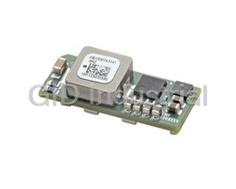
ABXS001A4X41-SRZ - BOOSTLYNX
ABXS002A3X41-SRZ - BOOSTLYNX
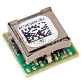
NON-ISOLATED DC/DC CONVERTERS 2.4-5.5VIN 3A 0.6-3.63VOUT
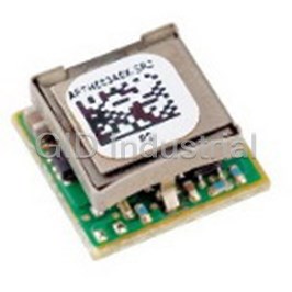
NON-ISOLATED DC/DC CONVERTERS SMT IN 2.4-5.5VDC OUT 0.59-3.63VDC 3A
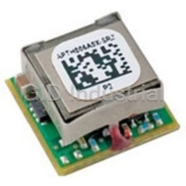
22 W, 2.4 -5.5 VDC Vin, Single Output, 3.3 VDC@6.0 A Industrial DC-DC Converter
NON-ISOLATED DC/DC CONVERTERS SMT IN 2.4-5.5VDC OUT 0.59-3.63VDC 6A
Request a Quote

The quote request has been received
Close

Facing challenges or have inquiries? Feel free to contact us!
Call Us +1-469-283-2440
What they say about us
FANTASTIC RESOURCE
One of our top priorities is maintaining our business with precision, and we are constantly looking for affiliates that can help us achieve our goal. With the aid of GID Industrial, our obsolete product management has never been more efficient. They have been a great resource to our company, and have quickly become a go-to supplier on our list!
Bucher Emhart Glass
EXCELLENT SERVICE
With our strict fundamentals and high expectations, we were surprised when we came across GID Industrial and their competitive pricing. When we approached them with our issue, they were incredibly confident in being able to provide us with a seamless solution at the best price for us. GID Industrial quickly understood our needs and provided us with excellent service, as well as fully tested product to ensure what we received would be the right fit for our company.
Fuji
HARD TO FIND A BETTER PROVIDER
Our company provides services to aid in the manufacture of technological products, such as semiconductors and flat panel displays, and often searching for distributors of obsolete product we require can waste time and money. Finding GID Industrial proved to be a great asset to our company, with cost effective solutions and superior knowledge on all of their materials, it’d be hard to find a better provider of obsolete or hard to find products.
Applied Materials
CONSISTENTLY DELIVERS QUALITY SOLUTIONS
Over the years, the equipment used in our company becomes discontinued, but they’re still of great use to us and our customers. Once these products are no longer available through the manufacturer, finding a reliable, quick supplier is a necessity, and luckily for us, GID Industrial has provided the most trustworthy, quality solutions to our obsolete component needs.
Nidec Vamco
TERRIFIC RESOURCE
This company has been a terrific help to us (I work for Trican Well Service) in sourcing the Micron Ram Memory we needed for our Siemens computers. Great service! And great pricing! I know when the product is shipping and when it will arrive, all the way through the ordering process.
Trican Well Service
GO TO SOURCE
When I can't find an obsolete part, I first call GID and they'll come up with my parts every time. Great customer service and follow up as well. Scott emails me from time to time to touch base and see if we're having trouble finding something.....which is often with our 25 yr old equipment.
ConAgra Foods