

 Manufacturers
MURATA POWER SOLUTIONS OKDL-T/60-W12-001-C

Description
Non-Isolated DC/DC Converters 60A DC-DC Converter LGA 0-1.8Vout Pos On
Part Number
OKDL-T/60-W12-001-C
Price
Request Quote
Manufacturer
MURATA POWER SOLUTIONS
Lead Time
Request Quote
Category
Capacitors » DC-DC Converter
Specifications
Manufacturer
Murata Power Solutions
Manufacturers Part #
OKDL-T/60-W12-001-C
Industry Aliases
Packaging
Tape and Reel
Series
OKDL-T/60-W12-xxx-C
Factory Pack Quantity
160
Application
Non-Isolated / Point-of-Load
Connection Type
Surface Mount
Dimensions
0.98 x 0.28 x 0.55"
Efficiency
92.90%
Environmental Conditions
General Purpose
Industry
Datacom, Industrial, OEM/Commercial
Input Voltage Nominal
12, 5
Mechanical Style
Non-Isolated / POL
Operating Temperature
-40 to +85°C, Full Load
Output Amps 1
60 A
Power
60A W
Subcategory
DC-DC Converter
Weight
7
Datasheet


Extracted Text
OKDL-T/60-W12-xxx-C 60A Digital PoL DC-DC Converter Series Typical units FEATURES PRODUCT OVERVIEW Input voltage range of 4.5 to 14Vdc The OKDL-T/60-W12 series are high efficiency, digital Apart from standard PoL performance and safety Point-of-Load (PoL) DC-DC power converters capable features like OVP, OCP, OTP, and UVLO, these 0.6 V - 1.8 V output voltage range digital converters have advanced features: digital of delivering 60A/108W. Available in a Land Grid High efficiency, typ. 94.9% at 5Vin, current sharing (full power, no derating), non-linear Array Package, these converters have a typical 1.8Vout half-load transient response, optimized dead time control, efficiency of 94.9%. PMBus™ compatibility allows LGA Package: 25.1 x 14.1 x 7.0 mm synchronization, and phase spreading. These monitoring and configuration of critical system-level (0.99 x 0.556 x 0.276 in) converters are ideal for use in telecommunications, performance requirements. networking, and distributed power applications. Configuration & Monitoring via PMBus™ Synchronization & phase spreading Current sharing, Voltage Tracking & Voltage margining Power Management via PMBus™ Applications MTBF 50 Mhrs Configurable soft-start/stop Distributed power architectures Non-Linear Response for reduction of Intermediate bus voltage applications Configurable output voltage (Vout) and voltage decoupling capacitor margins (Margin low and Margin high) Servers and storage applications Remote On/Off control & Power Good Configurable protection limits for OVP, input over Network equipment Output short-circuit, output over voltage, input under voltage, over current, on/off, voltage, & over temperature protection and temperature Certified to UL/IEC 60950-1 Status monitor Vout, Iout, Vin, Temp, Power Good, and On/Off PART NUMBER STRUCTURE OKD L - T / 60 – W12 - xxx - CC Digital Non-isolated PoL RoHS Hazardous Substance Compliance C = RoHS-6 (does not claim EU RoHS exemption 7b – lead in solder) L = Land Grid Array (LGA) Software Configuration Digits Trimmable Output (001 is positive turn-on logic) Voltage Range (002 is negative turn-on logic)* 0.6 - 1.8Vdc *Special quantity order is required; Maximum Rated Output contact Murata Power Solutions for Input Voltage Range Current in Amps MOQ and lead times. 4.5-14Vdc www.murata-ps.com/support MDC_OKDL-T/60-W12-xxx-C.A02 Page 1 of 73 OKDL-T/60-W12-xxx-C 60A Digital PoL DC-DC Converter Series Ordering Guide Model Number Package Type Output Input Range On/Off Logic OKDL-T/60-W12-001-C Land Grid Array 0.6-1.8V, 60A/108W 4.5V to 14V Positive Absolute Maximum Ratings Characteristics Min Typ Max Unit T Operating temperature (see Thermal Consideration section) -40 150 °C P1 T Storage temperature (Ambient) -40 125 °C S Input voltage (See Operating Information Section for input VI -0.3 16 V Signal I/O voltage CTRL, SA0, SA1, SALERT, SCL, SDA, VSET, SYNC, PG, VTRK -0.3 6.5 V Ground voltage -S, PREF, GND -0.3 0.3 V differential Analog pin voltage VO, +S -0.3 6.5 V General and Safety Conditions Min Typ Max Unit Safety Designed for UL/IEC/EN 60950 1 Calculated MTBF Telcordia SR-332, Issue 2 Method 1 50.15 Mhrs Stresses above those listed under Absolute Maximum Ratings may cause permanent damage to the device. This is a stress rating only; functional operation of the device at these or any other conditions above those indicated in the Electrical Specification section of this specification is not implied. Exposure to absolute maximum rating conditions for extended periods may affect device reliability. Configuration File This product is designed with a digital control circuit. The control circuit uses a configuration file which determines the functionality and performance of the product. The Electrical Specification table shows parameter values of functionality and performance with the Standard configuration, unless otherwise specified. The Standard configuration is designed to fit most application needs. Changes in Standard configuration might be required to optimize performance in specific application. Note that current sharing operation requires changed configuration. www.murata-ps.com/support MDC_OKDL-T/60-W12-xxx-C.A02 Page 2 of 73 OKDL-T/60-W12-xxx-C 60A Digital PoL DC-DC Converter Series Product Electrical Specifications OKDL-T/60-W12-xxx-C T = -30 to +95 °C, V = 4.5 to 14 V, unless otherwise specified under Conditions. P1 I Typical values given at: T = +25 °C, V = 12.0 V, max I , unless otherwise specified under Conditions. P1 I O VO defined by pin strap. Standard configuration. Tested with external CIN = 470 μF/10 mΩ + 8 x 47 μF, COUT = 10 x 470 μF/5 mΩ + 10 x 100 μF. See Operating Information section for design of input and output filters for a specific application. In the test set-up sense lines are connected directly to output pins on a converter and all the output voltage measurements are made on output pins. Characteristics Conditions Min Typ Max Unit Input voltage 4.5 14 V VI Input voltage slew rate Monotonic 2.4 V/ms Output voltage without pin-strap 1.2 V Output voltage adjustment range 0.60 1.8 V Output voltage adjustment including PMBus 0.54 1.98V margining Output voltage set-point resolution ±1.2 mV Including line, load, temp -1 1 % VO Output voltage accuracy Current sharing. Note 2 -2 2 % VO Internal resistance +S/-S to VOUT/GND 47 Ω V O +S bias current 110 μA -S bias current -110 μA VO = 0.6 V 1 Line regulation I = max I V = 1.0 V 1 mV O O O V = 1.8 V 1 O V = 0.6 V 1 O Load regulation I = 0 - 100% V = 1.0 V 1 mV O O V = 1.8 V 1 O V = 0.6 V 6 O Output ripple & noise V V = 1.0 V 7 mVp-p Oac O (up to 20 MHz) V = 1.8 V 9 O I Output current 0 60 A O I Current limit threshold 62 72 80 A lim RMS, hiccup mode, Isc Short circuit current 9 A V = 1.0 V, 6 mΩ short O V = 0.6 V 87.6 O 50% of max I V = 1.0 V 90.8 % O O V = 1.8 V 93.6 O η Efficiency V = 0.6 V 83.9 O I = max I V = 1.0 V 88.3 % O O O V = 1.8 V 92.0 O VO = 0.6 V 6.9 Pd Power dissipation at max IO VO = 1.0 V 7.9 W VO = 1.8 V 9.4 VO = 0.6 V 0.86 Pli Input idling power IO = 0 VO = 1.0 V 1.0 W VO = 1.8 V 1.6 Turned off with CTRL-pin 180 mW P Input standby power CTRL Low power mode 90 mW CI Internal input capacitance VI = 0 V 132 μF CO Internal output capacitance VO = 0 V 500 μF Total external output capacitance Note 3 1000 35000 uF COUT ESR range of external capacitors Per single capacitor. Note 3 3 30 mΩ Note 1. For Vout < 1.0V accuracy is ±10 mV. For further deviations see section Output Voltage Adjust using PMBus. Note 2. Accuracy here means deviation from ideal output voltage level given by configured droop and actual load. Includes line, load and temp variations. Note 3. This range applies to the “Universal PID” setting described in Operating Information. www.murata-ps.com/support MDC_OKDL-T/60-W12-xxx-C.A02 Page 3 of 73 OKDL-T/60-W12-xxx-C 60A Digital PoL DC-DC Converter Series Common Electrical Specifications This section includes parameter specifications common to all product versions within the product series. Typically these are parameters defined by the digital controller of the products. In the table below PMBus commands for configurable parameters are written in capital letters. T = -30 to +95 °C, V = 4.5 to 14 V, VI > V + 1.0 V unless otherwise specified under Conditions. P1 I O Typical values given at: T = +25 °C, V = 12.0 V, max I , unless otherwise specified under Conditions. P1 I O VO defined by pin-strap. Standard configuration. Characteristics Conditions Min Typ Max Unit Switching Frequency 320 kHz PMBus configurable Switching Frequency Range, Note 1 200 640 kHz FREQUENCY_SWITCH Switching Frequency Set-point Accuracy -5 5 % f = 1/T SW SW External Sync Duty Cycle 95 - % External Sync Pulse Width 150 ns Input Clock Frequency Drift Tolerance External sync -13 13 % TINIT Initialization Time From VI > ~3 V to ready to be enabled 50 ms Enable by input voltage TINIT + TONdel Output voltage T ONdel_tot Total On Delay Time Enable by CTRL pin TONdel Turn on delay duration 5 ms Turn off delay duration 5 ms Output voltage Accuracy (actual delay vs set value) -0.25/+4 ms T ONdel On Delay Time Range PMBus configurable 0 200 ms TOFF_DELAY Delay accuracy (actual delay vs set value) -0/+2 ms Turn on ramp duration 5 ms Disabled in standard configuration. Turn off immediately Turn off ramp duration upon expiration of Turn off delay. Output voltage T / On/Off Ramp duration range ONrise TOFFfall Ramp Time PMBus configurable 0 200 ms (0-100%-0 of VO) TON_RISE/TOFF_FALL 100 μs Ramp time accuracy for standalone operation (actual ramp time vs set value) Current sharing 20% of set value Characteristics Conditions Min Typ Max Unit Rising 90 %V O PG threshold Falling 85 %V O PMBus configurable PG thresholds range POWER_GOOD_ON 0 100 %V O Power Good, PG VOUT_UV_FAULT_LIMIT From VO reaching target to PG PG delay 50-200 ms assertion PMBus configurable PG delay range 0 5000 ms POWER_GOOD_DELAY IUVP threshold 3.85 V PMBus configurable IUVP threshold range 3.85 14 V VIN_UV_FAULT_LIMIT IUVP hysteresis 0.35 V Input Under Voltage Protection, PMBus configurable IUVP hysteresis range 0 10.15 V IUVP VIN_UV_WARN_LIMIT Set point accuracy -150 +150 mV IUVP response delay 2.5 μs VIN_UV_FAULT_RESPONSE Fault response Automatic restart, 70 ms. Note 2 www.murata-ps.com/support MDC_OKDL-T/60-W12-xxx-C.A02 Page 4 of 73 OKDL-T/60-W12-xxx-C 60A Digital PoL DC-DC Converter Series Characteristics Conditions Min Typ Max Unit IOVP threshold 16 V PMBus configurable IOVP threshold range 4.2 16 V VIN_OV_FAULT_LIMIT IOVP hysteresis 1 V Input Over Voltage Protection, PMBus configurable IOVP hysteresis range 0 11.8 V IOVP VIN_OV_WARN_LIMIT Set point accuracy -150 +150 mV IOVP response delay 2.5 μs Fault response VIN_OV_FAULT_RESPONSE Automatic restart, 70 ms. Note 2 UVP threshold 85 % V O PMBus configurable UVP threshold range 0 100 %VO VOUT_UV_FAULT_LIMIT Output Voltage OVP threshold 115 % V O Over/Under Voltage PMBus configurable Protection, OVP threshold range 100 115 %V O VOUT_OV_FAULT_LIMIT OVP/UVP UVP/OVP response time 25 μs VOUT_UV_FAULT_RESPONSE Fault response Automatic restart, 70 ms. Note 2 VOUT_OV_FAULT_RESPONSE OCP threshold Set value 76 A Over Current Protection, PMBus configurable OCP threshold range 0-76 A IOUT_AVG_OC_FAULT_LIMIT OCP Protection delay PMBus configurable 1-32 TSW Fault response MFR_IOUT_OC_FAULT_RESPONSE Automatic restart, 70 ms. Note 2 OTP threshold 125 C Over Temperature PMBus configurable Protection, OTP threshold range -40 +125 C OT_FAULT_LIMIT OTP Position P4 OTP hysteresis PMBus configurable 15 C Fault response OT_FAULT_RESPONSE Automatic restart, 240 ms. Note 2 www.murata-ps.com/support MDC_OKDL-T/60-W12-xxx-C.A02 Page 5 of 73 OKDL-T/60-W12-xxx-C 60A Digital PoL DC-DC Converter Series Characteristics Conditions Min Typ Max Unit Input voltage ±3 %VI READ_VIN Output voltage ±1 %VO READ_VOUT TP1 = 25 C, VO = 1.0 V ±3 A Output current Monitoring Accuracy READ_IOUT ±5 A TP1 = 0 - 95 C, VO = 1.0 V Duty cycle < 10% -3 3 % Duty cycle READ_DUTY_CYCLE Duty cycle > 10% -1 ±0.5 1 % Temperature Position P4 -5 5 °C READ_TEMPERATURE_1 Tracking Input Bias Current VTRK pin 110 200 μA Tracking Input Voltage Range VTRK pin 0 5 V Regulation 100% tracking -1 1 % Tracking Accuracy Ramp accuracy, VO = 1.0 V, 10 ms ramp -100 100 mV Current difference between products in a current sharing Steady state operation Max 2 x READ_IOUT monitoring accuracy group Number of products in a current sharing group 8 V Logic output low signal level 0.8 V OL SCL, SDA, SYNC, GCB, SALERT, PG Sink / source current = 4 mA V Logic output high signal level 2.25 V OH I Logic output low sink current 4 mA OL I Logic output high source current 2 mA OH V Logic input low threshold 0.8 V IL SCL, SDA, CTRL, SYNC, GCB VIH Logic input high threshold 2 V II_LEAK Logic leakage current SCL, SDA, SYNC, SALERT, PG 10 μA CI_PIN Logic pin input capacitance SCL, SDA, CTRL, SYNC, GCB 10 pF SCL, SDA, SALERT No internal pull-up R Logic pin internal pull-up resistance I_PU CTRL to +5V 1 kΩ fSMB SMBus Operating frequency 100 kHz STOP bit to START bit T SMBus Bus free time 2 ms BUF See section SMBus – Timing tset SMBus SDA setup time from SCL See section SMBus – Timing 300 ns t SMBus SDA hold time from SCL See section SMBus – Timing 250 ns hold Note 1.There are configuration changes to consider when changing the switching frequency, see section Switching Frequency. Changing switching frequency below 320 kHz is not recommended for Vout > 1.2V. Note 2.Automatic restart ~70 ms or 240 ms after fault if the fault is no longer present. Continuous restart attempts if the fault reappear after restart. See Operating Information for other fault response options. Note 3.The typical initialization time varies in the range ~40-50 ms, depending on the On Delay Time (TON_DELAY) and On Ramp Time (TON_RISE) settings. www.murata-ps.com/support MDC_OKDL-T/60-W12-xxx-C.A02 Page 6 of 73 OKDL-T/60-W12-xxx-C 60A Digital PoL DC-DC Converter Series Typical Output Characteristics, V = 0.6 V O Standard configuration unless otherwise specified,T =+25 °C P1 Power Dissipation Efficiency [%] [W] 10 95 90 8 V V I I 85 6 4,5 V 4,5V 80 5 V 5 V 4 12 V 75 12 V 14 V 2 14 V 70 0 65 0 102030 405060 0 1020304050 60 [A] [A] Efficiency vs. load current and input voltage. Dissipated power vs. load current and input voltage. Output Current Derating Load Regulation [A] [V] 70 0.606 60 0.604 3.0 m/s 50 2.0 m/s 4.5 V 0.602 40 5.0 V 1.0 m/s 0.600 30 12 V 0.5 m/s 0.598 14 V 20 Nat. Conv. 10 0.596 0 0.594 50 60 70 80 90 100 110 120 [°C] 0 102030 405060 [A] Available load current vs. ambient air temperature and airflow at Output voltage vs load current. V = 12 V. See section Thermal Consideration. I Output Ripple and Noise Transient Response Fundamental output voltage ripple at V = 12 V, I = 60 A, Output voltage response to load current step change (15–45–15 A), I O C = 3 x 470 μF/4.5 mΩ + 10 x 100 μF di/dt = 2 A/µs, at V = 12 V, C = 6 x 470 μF/4.5 mΩ + 10 x 100 μF. OUT I OUT Scale: 5 mV/div, 2 µs/div, 20 MHz bandwidth. Compensation settings by DLC and optimized NLR. See section Output Ripple and Noise. Scale: 50 mV/div, 20 A/div, 200 µs/div. www.murata-ps.com/support MDC_OKDL-T/60-W12-xxx-C.A02 Page 7 of 73 OKDL-T/60-W12-xxx-C 60A Digital PoL DC-DC Converter Series Typical Output Characteristics, V = 1.0 V O Standard configuration unless otherwise specified,TP1=+25 °C Efficiency Power Dissipation [%] [W] 95 10 90 8 V V I I 4.5 V 85 6 4.5V 5 V 5 V 80 4 12 V 12 V 14 V 75 2 14 V 70 0 0 1020 30405060 0 1020304050 60 [A] [A] Efficiency vs. load current and input voltage. Dissipated power vs. load current and input voltage. Output Current Derating Load Regulation [A] [V] 70 1.010 60 3.0 m/s 1.005 50 2.0 m/s 4.5 V 40 1.0 m/s 5.0 V 1.000 30 12 V 0.5 m/s 14 V 20 Nat. Conv. 0.995 10 0 0.990 50 60 70 80 90 100 110 120 [°C] 0 102030 405060 [A] Available load current vs. ambient air temperature and airflow at Output voltage vs load current. V = 12 V. See section Thermal Consideration. I Output Ripple and Noise Transient Response Fundamental output voltage ripple at V = 12 V,I = 60 A, Output voltage response to load current step change (15–45–15 A), I O C = 3 x 470 μF/4.5 mΩ + 10 x 100 μF di/dt = 2 A/µs, at V = 12 V, C = 6x470 μF/4.5 mΩ + 10x100 μF. OUT I OUT Scale: 5 mV/div, 2 µs/div, 20 MHz bandwidth. Compensation settings by DLC and optimized NLR. See section Output Ripple and Noise. Scale: 50 mV/div, 20 A/div, 200 µs/div. www.murata-ps.com/support MDC_OKDL-T/60-W12-xxx-C.A02 Page 8 of 73 OKDL-T/60-W12-xxx-C 60A Digital PoL DC-DC Converter Series Typical Output Characteristics, V = 1.8 V O Standard configuration unless otherwise specified,TP1=+25 °C Efficiency Power Dissipation [%] [W] 100 12 95 10 V V I I 90 8 4,5 V 4,5V 85 6 5 V 5 V 12 V 80 4 12 V 14 V 14 V 2 75 70 0 0 1020 30405060 0 1020304050 60 [A] [A] Efficiency vs. load current and input voltage. Dissipated power vs. load current and input voltage. Output Current Derating Load Regulation [A] [V] 70 1.820 60 3.0 m/s 1.810 50 2.0 m/s 4.5 V 40 1.0 m/s 5.0 V 1.800 30 12 V 0.5 m/s 14 V 20 Nat. Conv. 1.790 10 0 1.780 50 60 70 80 90 100 110 120 [°C] 0 102030 405060 [A] Available load current vs. ambient air temperature and airflow at Output voltage vs load current. V = 12 V. See section Thermal Consideration. I Output Ripple and Noise Transient Response Fundamental output voltage ripple at V = 12 V,I = 60 A, Output voltage response to load current step change (15–45–15 A), I O C = 3 x 470 μF/4.5 mΩ + 10 x 100 μF di/dt = 2 A/µs, at V = 12 V, C = 6 x 470 μF/4.5 mΩ + 10 x 100 μF. OUT I OUT Scale: 5 mV/div, 2 µs/div, 20 MHz bandwidth. Compensation settings by DLC and optimized NLR. See section Output Ripple and Noise. Scale: 50 mV/div, 20 A/div, 200 µs/div. www.murata-ps.com/support MDC_OKDL-T/60-W12-xxx-C.A02 Page 9 of 73 OKDL-T/60-W12-xxx-C 60A Digital PoL DC-DC Converter Series Typical On/Off Characteristics Standard configuration, T = +25 °C, V = 1.0 V P1 O Enable by input voltage – PG Open-Drain (default) Disable by input voltage – PG Open-Drain (default) V I V I V V O O PG PG Output enabled by applying V . V = 12 V, I = max I . Output disabled by removing V . V = 12 V, I = max I . I I O O I I O O TON_DELAY = TON_RISE = 5 ms, PG delay controlled by DLC. Scale from top: 10, 0.5, 2 V/div, 20 ms/div. MFR_CONFIG = 0x7F10 (default). PG pulled up to external voltage. Note: PG being high before Vin applied can be avoided by pulling up PG to Vout. Scale from top: 10, 0.5, 2 V/div, 20 ms/div. Enable by input voltage – PG Push-Pull Disable by input voltage – PG Push-Pull V I V I V V O O PG PG Output enabled by applying V . V = 12 V, I = max I . Output disabled by removing V . V = 12 V, I = max I . I I O O I I O O TON_DELAY = TON_RISE = 5 ms, POWER_GOOD_DELAY = 2 ms. Scale from top: 10, 0.5, 2 V/div, 20 ms/div. MFR_CONFIG = 0x7F12 (PG push-pull). Scale from top: 10, 0.5, 2 V/div, 20 ms/div. Enable by CTRL pin Disable by CTRL pin CTRL CTRL V O V O PG PG Output enabled by CTRL pin. V = 12 V, I = max I . Output disabled by CTRL pin. V = 12 V, I = max I I O O I O O. TON_DELAY = TON_RISE = 5 ms, PG delay controlled by DLC. Scale from top: 5, 0.5, 2 V/div, 10 ms/div. Scale from top: 5, 0.5, 2 V/div, 20 ms/div. www.murata-ps.com/support MDC_OKDL-T/60-W12-xxx-C.A02 Page 10 of 73 OKDL-T/60-W12-xxx-C 60A Digital PoL DC-DC Converter Series Typical Charactersitics Standard configuration, T = +25 °C P1 Efficiency vs. Output Current and Power Dissipation vs. Output Current and Switching Frequency Switching Frequency [%] [W] 95 12 10 90 200 kHz 200 kHz V V I I 8 85 320 kHz 320 kHz 6 80 480 kHz 480 kHz 4 75 640 kHz 640 kHz 2 70 0 0 102030 405060 0 102030 405060 [A] [A] Efficiency vs. load current and switching frequency at Dissipated power vs. load current and switching frequency at V = 12 V, V = 1.0 V, C = 3 x 470 μF/4.5 mΩ + 10 x 100 μF. V = 12 V, V = 1.0 V, C = 3 x 470 μF/4.5 mΩ + 10 x 100 μF. I O OUT I O OUT Frequency changed by PMBus command FREQUENCY_SWITCH. Frequency changed by PMBus command FREQUENCY_SWITCH. Output Ripple vs. Switching Frequency [mV ] pk-pk 16 12 V O 0.6 V 8 1.0 V 4 1.8 V 0 200 300 400 500 600 [kHz] Output voltage ripple V vs. switching frequency at pk-pk V = 12 V, I = max I , C = 3 x 470 μF/4.5 mΩ + 10 x 100 μF. I O O OUT Frequency changed by PMBus command FREQUENCY_SWITCH. www.murata-ps.com/support MDC_OKDL-T/60-W12-xxx-C.A02 Page 11 of 73 OKDL-T/60-W12-xxx-C 60A Digital PoL DC-DC Converter Series EMC Specification Output Ripple and Noise Conducted EMI is measured according to the test set-up below. The typical Output ripple and noise are measured according to figure below. A 50 mm fundamental switching frequency is 320 kHz. conductor works as a small inductor forming together with the two capacitances a damped filter. Conducted EMI Input terminal value (typical for standard configuration). V = 12 V, V = 1.0 V, I O 50 mm conductor I = 60 A. O Vout Tantalum Ceramic Capacitor Capacitor S c o 10 µF 0.1 µF S GND 50 mm conductor BNC-contact to oscilloscope Output ripple and noise test set-up. The digital compensation of the product is designed to automatically provide stability, accurate line and load regulation and good transient performance for a wide range of operating conditions (switching frequency, input voltage, output voltage, output capacitance). Inherent from the implementation and normal to the product there will be some low frequency ripple at the output, in addition to the fundamental switching frequency output ripple. This low frequency ripple is not related to instability of control loop. The total output ripple and noise is maintained at a low level. EMI without filter. V =12 V, V =1.0 V, I =60 A, C = 10 x 100 μF + 3 x 470 μF/4.5 mΩ, 5 mV/div, 50 μs/div I O O OUT Example of low frequency ripple at the output. Test set-up conducted emission, power lead. 2 DUT = Product mounted on a 154 cm test board with the external capacitances CIN = 470 μF/10 mΩ + 8 x 47 μF and COUT = 3 x 470 μF/4.5 mΩ + 10 x 100 μF. www.murata-ps.com/support MDC_OKDL-T/60-W12-xxx-C.A02 Page 12 of 73 Load OKDL-T/60-W12-xxx-C 60A Digital PoL DC-DC Converter Series PMBus Interface Index RSA [k] Index RSA [k] 0 10 13 34.8 Power Management Overview 1 11 14 38.3 This product incorporates a wide range of configurable power management features that are simple to implement with a minimum of external 2 12.1 15 42.2 components. Additionally, the product includes protection features that 3 13.3 16 46.4 continuously safeguard the load from damage due to unexpected system 4 14.7 17 51.1 faults. 5 16.2 18 56.2 The product’s standard configuration is suitable for a wide range of 6 17.8 19 61.9 operation in terms of input voltage, output voltage, and load. The configuration is stored in an internal Non-Volatile Memory (NVM). All power 7 19.6 20 68.1 management functions can be reconfigured using the PMBus interface. 8 21.5 21 75 9 23.7 22 82.5 Throughout this document, different PMBus commands are referenced. A detailed description of each command is provided in the appendix at the 10 26.1 23 90.9 end of this specification. 11 28.7 24 100 12 31.6 SMBus Interface 2 The product can be used with any standard two-wire I C or SMBus host The PMBus address follows the equation below: device. See Electrical Specification for allowed clock frequency range. In addition, the product is compatible with PMBus version 1.1 and includes an PMBus Address (decimal) = 25 x (SA1 index) + (SA0 index) SALERT line to help mitigate limitations related to continuous fault monitoring. The product supports 100 kHz bus clock frequency only. The The user can theoretically configure up to 625 unique PMBus addresses, PMBus signals SCL, SDA and SALERT require passive pull-up resistors as however the PMBus address range is inherently limited to 128. Therefore, stated in the SMBus Specification. Pull-up resistors are required to the user should use index values 0 - 4 on the SA1 pin and the full range of guarantee the rise time as follows: index values on the SA0 pin, which will provide 125 device address combinations. Note that address 0x4B is allocated for production needs and R C 1s P p cannot be used. where Rp is the pull-up resistor value and Cp is the bus loading. The Alternatively the PMBus address can be defined by connecting the SA0/SA1 maximum allowed bus load is 400 pF. The pull-up resistor should be tied to pins according to the table below. SA1 = open for products with no SA1 pin. an external supply voltage in range from 2.5 to 5.5 V, which should be present prior to or during power-up. If the proper power supply is not SA0 available, voltage dividers may be applied. Note that in this case, the resistance in the equation above corresponds to parallel connection of the Low Open High resistors forming the voltage divider. Low 20h 21h 22h SA1 Open 23h 24h 25h PMBus Addressing The PMBus address should be configured with resistors connected High 26h 27h Reserved between the SA0/SA1 pins and the PREF pin, as shown in the Typical Application Circuit. Recommended resistor values for hard-wiring PMBus Low = Shorted to PREF addresses are shown in the table below. 1% tolerance resistors are Open = High impedance required. High = Logic high, GND as reference, Logic High definitions see Electrical Specification Reserved Addresses Addresses listed in the table below are reserved or assigned according to the SMBus specification and may not be usable. Refer to the SMBus specification for further information. www.murata-ps.com/support MDC_OKDL-T/60-W12-xxx-C.A02 Page 13 of 73 OKDL-T/60-W12-xxx-C 60A Digital PoL DC-DC Converter Series Fault & Warning Status PMBus Command Address Comment STATUS_WORD Overview, Power Good 0x00 General Call Address / START byte STATUS_BYTE 0x01 CBUS address Output voltage level STATUS_VOUT 0x02 Address reserved for different bus format Output current level STATUS_IOUT 0x03 - 0x07 Reserved for future use Input voltage level STATUS_INPUT 0x08 SMBus Host Temperature level STATUS_TEMPERATURE 0x09 - 0x0B Assigned for Smart Battery PMBus communication STATUS_CML 0x0C SMBus Alert Response Address Miscellaneous STATUS_MFR_SPECIFIC 0x28 Reserved for ACCESS.bus host Reserved by previous versions of the SMBus Snapshot Parameter Capture 0x2C - 0x2D specification This product offers a special feature that enables the user to capture parametric data during normal operation by a single PMBus command 0x37 Reserved for ACCESS.bus default address SNAPSHOT. The following parameters are stored: Reserved by previous versions of the SMBus 0x40 - 0x44 specification Input voltage 0x48 - 0x4B Unrestricted addresses Output voltage 0x61 SMBus Device Default Address Output current Controller temperature 0x78 - 0x7B 10-bit slave addressing Switching frequency 0x7C - 0x7F Reserved for future use Duty cycle Status and fault information Monitoring via PMBus When a fault occurs the Snapshot functionality will automatically store this It is possible to continuously monitor a wide variety of parameters through parametric data to NVM. The data can then later be read back to provide the PMBus interface. These include, but are not limited to, the parameters valueable information for analysis. listed in the table below. 2 PMBus/I C Timing Parameter PMBus Command � �� Input voltage READ_VIN ��� � �� Output voltage READ_VOUT Total output current READ_IOUT � �� ��� Controller temperature READ_TEMPERATURE_1 � �� Switching frequency READ_FREQUENCY � � Duty cycle READ_DUTY_CYCLE ��� ���� Setup and hold times timing diagram. Monitoring Faults The setup time, tset, is the time data, SDA, must be stable before the rising Fault conditions can be monitored using the SALERT pin, which will be edge of the clock signal, SCL. The hold time t , is the time data, SDA, hold asserted low when any number of pre-configured fault or warning must be stable after the falling edge of the clock signal, SCL. If these times conditions occur. The SALERT pin will be held low until faults and/or are violated incorrect data may be captured or meta-stability may occur and warnings are cleared by the CLEAR_FAULTS command, or until the output the bus communication may fail. All standard SMBus protocols must be voltage has been re-enabled. followed, including clock stretching. Refer to the SMBus specification, for SMBus electrical and timing requirements. In response to the SALERT signal, the user may read a number of status commands to find out what fault or warning condition occurred, see table This product does not support the BUSY flag in the status commands to below. indicate product being too busy for SMBus response. Instead a bus-free time delay according to this specification must occur between every SMBus transmission (between every stop & start condition). The product supports PEC (Packet Error Checking) according to the SMBus specification. When sending subsequent commands to the same module, it is recommended to insert additional delays according to the table below. www.murata-ps.com/support MDC_OKDL-T/60-W12-xxx-C.A02 Page 14 of 73 OKDL-T/60-W12-xxx-C 60A Digital PoL DC-DC Converter Series Initialization Procedure Required delay before The product follows an internal initialization procedure after power is applied After sending PMBus Command additional command to the VIN pins: STORE_USER_ALL 1. Self test and memory check. 100 ms STORE_DEFAULT_ALL 2. The address pin-strap resistors are measured and the associated PMBus address is defined. RESTORE_USER_ALL 100 ms RESTORE_DEFAULT_ALL 3. The output voltage pin-strap resistor is measured and the associated output voltage level will be loaded to operational RAM of PMBus command 10 ms VOUT_MAX VOUT_COMMAND. 2 ms after reading Any other command 10 ms after writing 4. Factory default values stored in default NVM memory are loaded to operational RAM. This overwrites any previously loaded values. Non-Volatile Memory (NVM) 5. Values stored in the User NVM are loaded into operational RAM memory. The product incorporates two Non-Volatile Memory areas for storage of the This overwrites any previously loaded values (e.g. VOUT_COMMAND by PMBus command values; the Default NVM and the User NVM. pin-strap). The Default NVM is pre-loaded with factory default values. The Default NVM is 6. Check for external clock signal at the SYNC pin and lock internal clock to write-protected and can be used to restore the factory default values through the external clock if used. the command RESTORE_DEFAULT_ALL. Once this procedure is completed and the Initialization Time has passed (see Electrical Specification), the output voltage is ready to be enabled using the CTRL pin. The product is also ready to accept commands via the PMBus interface, which in case of writes will overwrite any values loaded during the initialization procedure. INITIALIZATION Pin-strap resistors INITIALIZATION Default NVM Factory default RESTORE_DEFAULT_ALL Write-protected RAM INITIALIZATION User NVM Factory default STORE_USER_ALL Customizable RESTORE_USER_ALL WRITE Illustration of Initialization time. PMBus interface READ Illustration of memory areas of the product. The User NVM is pre-loaded with factory default values. The User NVM is writable and open for customization. The values in NVM are loaded during initialization according to section Initialization Procedure, whereafter commands can be changed through the PMBus Interface. The STORE_USER_ALL command will store the changed parameters to the User NVM. Command Protection The user may write-protect specific PMBus commands in the User NVM by using the command UNPROTECT. www.murata-ps.com/support MDC_OKDL-T/60-W12-xxx-C.A02 Page 15 of 73 OKDL-T/60-W12-xxx-C 60A Digital PoL DC-DC Converter Series Operating Information For most applications non-tantalum capacitors are preferred due to the robustness of such capacitors to accommodate high inrush currents of systems being powered from very low impedance sources. It is Input Voltage recommended to use a combination of ceramic capacitors and low-ESR The input voltage range 4.5-14V makes the product electrolytic/polymer bulk capacitors. The low ESR of ceramic capacitors easy to use in intermediate bus applications when powered effectively limits the input ripple voltage level, while the bulk capacitance by a non-regulated bus converter or a regulated bus converter. minimizes deviations in the input voltage at large load transients. Input Under Voltage Protection (IUVP) If several products are connected in a phase spreading setup the amount of The product monitors the input voltage and will turn-on and turn-off at input ripple current, and capacitance per product, can be reduced. Input configured thresholds (see Electrical Specification). The turn-on input capacitors must be placed closely and with low impedance connections to voltage threshold is set higher than the corresponding turn-off threshold. the VIN and GND pins in order to be effective. Hence, there is a hysteresis between turn-on and turn-off input voltage levels. Once the input voltage falls below the turn-off threshold, the device External Output Capacitors can respond in several ways as follows: The output capacitor requirement depends on two considerations; output 1. Immediate and definite shutdown of output voltage until the fault is ripple voltage and load transient response. To achieve low ripple voltage, cleared by PMBus command CLEAR_FAULTS or the output voltage is the output capacitor bank must have a low ESR value, which is achieved re-enabled. with ceramic output capacitors. A low ESR value is critical also for a small output voltage deviation during load transients. Designs with smaller load 2. Immediate shutdown of output voltage while the input voltage is transients can use fewer capacitors and designs with more dynamic load below the turn-on threshold. Operation resumes automatically and the content will require more load capacitors to achieve a small output output is enabled when the input voltage has risen above the turn-on deviation. Improved transient response can also be achieved by adjusting threshold. the settings of the control loop of the product. Adding output capacitance decreases loop band-width. 3. Continue operating for a given delay period, followed by shutdown if the fault still exists. The device will remain in shutdown until the It is recommended to locate low ESR ceramic and low ESR output voltage is re-enabled. electrolytic/polymer capacitors as close to the load as possible, using The response for the standard configuration is option 2. The IUVP function several capacitors in parallel to lower the effective ESR. It is important to can be reconfigured using the PMBus commands VIN_UV_FAULT_LIMIT use low resistance and low inductance PCB layouts and cabling in order for (turn-off threshold), VIN_UV_WARN_LIMIT (turn-on threshold) and capacitance to be effective. VIN_UV_FAULT_RESPONSE. Control Loop Input Over Voltage Protection (IOVP) The product uses a voltage-mode synchronous buck controller with a fixed The product monitors the input voltage continously and will respond as frequency PWM scheme. Although the product uses a digital control loop, it configured when the input voltage rises above the configured threshold operates much like a traditional analog PWM controller. As in the analog level (see Electrical Specification). Refer to section “Input Under Voltage controller case, the control loop compares the output voltage to the desired Protection” for functionality, response configuration options and default voltage reference and compensation is added to keep the loop stable and setting. fast. The resulting error signal is used to drive the PWM logic. Instead of The IOVP function can be reconfigured using the PMBus commands using external resistors and capacitors required with traditional analog VIN_OV_FAULT_LIMIT (turn-off threshold), VIN_OV_WARN_LIMIT (turn-on control loops, the product uses a digital Proportional-Integral-Derivative threshold) and VIN_OV_FAULT_RESPONSE. (PID) compensator in the control loop. The characteristics of the control loop is configured by setting PID compensation parameters. These PID settings Input and Output Impedance can be reconfigured using the PMBus interface. The impedance of both the input source and the load will interact with the impedance of the product. It is important that the input source has low characteristic impedance. If the input voltage source contains significant inductance, the addition of a capacitor with low ESR at the input of the product will ensure stable operation. External Input Capacitors The input ripple RMS current in a buck converter can be estimated to I I D 1D inputRMS load Where I load is the output load current and D is the duty cycle. The maximum load ripple current becomes I /2. The ripple current is divided into three load parts, i.e., currents in the input source, external input capacitor, and internal input capacitor. How the current is divided depends on the impedance of the input source, ESR and capacitance values in the capacitors. www.murata-ps.com/support MDC_OKDL-T/60-W12-xxx-C.A02 Page 16 of 73 OKDL-T/60-W12-xxx-C 60A Digital PoL DC-DC Converter Series Control Loop Settings When saving changes to the user non-volatile memory, all changes made to Product variants without DLC have a standard configuration with a robust the content of RAM will be saved. This also includes the default PID setting control loop compensation setting (PID setting) which allows for a wide (loaded to RAM to act as a safe starting value) or the PID setting changed by range operation of input and output voltages and capacitive loads. For an the DLC algorithm after enabling output. The result is that as long as DLC is application with a specific input voltage, output voltage, and capacitive load, enabled the PID setting in the user non-volatile memory is ignored, but it the control loop can be optimized for a robust and stable operation and with might accidentally get overwritten. an improved load transient response. This optimization will minimize the amount of required output decoupling capacitors for a given load transient When changing DLC from disabled to enabled: requirement yielding an optimized cost and minimized board space. A non-configurable default PID setting is loaded to RAM to act as a safe starting value for the DLC (same as above). Dynamic Loop Compensation (DLC) This section applies to product variants with DLC (see section Ordering When changing DLC from enabled to disabled: Information). The DLC feature might in some documents be referred to as When changing DLC from enabled to disabled, the PID setting in the user “Auto Compensation” or “Auto Tuning” feature. non-volatile memory will be loaded to RAM. Any new optimized PID setting The DLC feature measures the characteristics of the power train and in RAM will be lost, if not first stored to the user non-volatile memory. calculates the proper compensator PID coefficients. The standard configuration is that once the output voltage ramp up has When DLC is disabled: completed, the DLC algorithm will begin and a new optimized compensator When DLC is disabled and input power has been applied, the PID setting in solution (PID setting) will be found and implemented. The DLC algorithm the user non-volatile memory will be loaded to RAM and used in the control typically takes between 50 ms and 200 ms to complete. loop. By the PMBus command AUTO_COMP_CONFIG the user may select The original PID setting in the user non-volatile memory is quite slow and between several different modes of operation: not recommended for optimal performance. If DLC is disabled it is Disable recommended to either: Autocomp once, will run DLC algorithm each time the output is 1. Use the DLC to find optimized PID setting. enabled (standard configuration) 2. Use Universal PID as defined below. Autocomp every second will initiate a new DLC algorithm each 1 The Universal PID setting (taps) is: second Autocomp every minute will initiate a new DLC algorithm every A = 1271.9, minute. B = -2309.9, C = 1045.2 The DLC can also be configured to run once only after the first ramp up Write 0x7B82A5FC905F7B9EFD to PID_TAPS register and write command (after input power have been applied) and to use that temporary stored PID STORE_USER_ALL settings in all subsequent ramps. If input power is cycled a new DLC Note that if DLC is enabled, for best results V must be stable before DLC I algorithm will be performed after the first ramp up. The default setting is algorithm begins. however to run the DLC algorithm after every ramp up. The DLC algorithm can also be initiated manually by sending the AUTO_COMP_CONTROL command. The DLC can also be configured with Auto Comp Gain Control. This scales the DLC results to allow a trade-off between transient response and steady- state duty cycle jitter. A setting of 100% will provide the fastest transient response while a setting of 10% will produce the lowest jitter. The default is 50%. Changing DLC and PID Setting Some caution must be considered while DLC is enabled and when it is changed from enabled or disabled. When operating, the controller IC uses the settings loaded in its (volatile) RAM memory. When the input power is applied the RAM settings are retrieved from the pin-strap resistors and the two non-volatile memories (DEFAULT and USER). The sequence is described in the “Initialization Procedure” section. When DLC is enabled: When DLC is enabled, the normal sequence (after input power has been applied) that a value stored in the user non-volatile memory overwrites any previously loaded value does not apply for the PID setting (stored in the PID_TAPS register). The PID setting in the user non-volatile memory is ignored and a non-configurable default PID setting is loaded to RAM to act as a safe starting value for the DLC. Once the output has been enabled and the DLC algorithm has found a new optimized PID setting, it will be loaded in RAM and used by the control loop. www.murata-ps.com/support MDC_OKDL-T/60-W12-xxx-C.A02 Page 17 of 73 OKDL-T/60-W12-xxx-C 60A Digital PoL DC-DC Converter Series Load Transient Response Optimization (NLR) The CTRL pin has an internal 10 kΩ pull-up resistor to 5 V. The external The product incorporates a Non-Linear transient Response, NLR, loop that device must provide a minimum required sink current to guarantee a decreases the response time and the output voltage deviation during a load voltage not higher than the logic low threshold level (see Electrical transient. The NLR results in a higher equivalent loop bandwidth than is Characteristics). When the CTRL pin is left open, the voltage generated on possible using a traditional linear control loop. The standard configuration the CTRL pin is max 5.5 V. has appropriate NLR settings for robust and stable operation for a wide range of input voltage and a capacitive load range as defined in the section If the device is to be synchronized to an external clock source, the clock External Decoupling Capacitors. For an application with a specific input frequency must be stable prior to enabling the output voltage. voltage, output voltage, and capacitive load, the NLR configuration can be optimized for a robust and stable operation and with an improved load Output Voltage Adjust using Pin-strap Resistor transient response. This will also reduce the amount of output decoupling Using an external Pin-strap resistor, RSET, the output voltage can be set to capacitors and yield a reduced cost. However, the NLR slightly reduces the several predefined levels shown in the table below. The resistor should be efficiency. In order to obtain maximal energy efficiency the load transient applied between the VSET pin and the PREF pin as shown in the Typical requirement has to be met by the standard control loop compensation and Application Circuit. Maximum 1% tolerance resistors are required. the decoupling capacitors. The NLR settings can be reconfigured using the PMBus interface. R [kΩ] V [V] R [kΩ] V [V] SET OUT SET OUT Remote Sense 0 (short) 0.60 26.1 1.10 The product has remote sense to compensate the voltage drops between the output and the point of load. The sense traces should be located close 10 0.60 28.7 1.15 to each other and to the PCB ground layer to reduce noise susceptibility. If 11 0.65 31.6 1.20 the remote sense is not needed +S must be connected to VOUT and −S 12.1 0.70 34.8 1.25 must be connected to GND. 13.3 0.75 38.3 1.30 In cases where the external output filter includes an inductor (forming a pi 14.7 0.80 42.2 1.40 filter) according to the picture below, the LEXT/CEXT resonant frequency 16.2 0.85 46.4 1.50 places an upper limit on the controller loop bandwidth. If the resonant frequency is high the sense lines can be connected after the filter (as shown 17.8 0.90 51.1 1.60 in the picture) – if the resonant frequency is low and the DC drop from LEXT 19.6 0.95 56.2 1.70 is acceptable, sensing before the filter may be better. 21.5 1.00 61.9 1.80 Vout L EXT 23.7 1.05 Infinite (open) 1.20 C C O EXT R also sets the maximum output voltage; see section Output Voltage SET GND Range Limitation. The resistor is sensed only during the initialization -S procedure after application of input voltage. Changing the resistor value +S during normal operation will not change the output voltage. See Ordering Information for output voltage range. External output filter with inductor (pi filter). Output Voltage Control To control the output voltage the following options are available: 1. Output voltage is controlled through the CTRL pin. 2. Output voltage is controlled using the PMBus command OPERATION. 3. Output voltage is controlled by CTRL pin and PMBus command OPERATION. 4. Output voltage is controlled to be “always on”. The CTRL pin can be used with active high (positive) logic or active low (negative) logic. The setting for the standard configuration is option 1, using positive logic. The output voltage control can be reconfigured using the PMBus command ON_OFF_CONFIG. www.murata-ps.com/support MDC_OKDL-T/60-W12-xxx-C.A02 Page 18 of 73 Load OKDL-T/60-W12-xxx-C 60A Digital PoL DC-DC Converter Series Output Voltage Adjust using PMBus Output Voltage Range Limitation The output voltage set by pin-strap can be overridden up to a certain level The output voltage range that is possible to set by configuration or by the (see section Output Voltage Range Limitation) by using the PMBus PMBus interface is hardware limited by the pin-strap resistor RSET. The command VOUT_COMMAND. See Electrical Specification for adjustment maximum output voltage is set to 110% of the output value defined by RSET. range. This protects the application circuit from an over voltage due to an accidental PMBus command. For current sharing (parallel) operation, VOUT_COMMAND should not be The limitation applies to the actual regulated output voltage rather than to used to change the output voltage on-the-fly. Instead broadcast voltage the configured value. Thus, it is possible to write and read back a margining should be used. See sections Voltage Margining Up/Down and VOUT_COMMAND value higher than the limit, but the actual output voltage Broadcast Control for details. will be limited. Note that for product variants with DLC (see Ordering Information) broadcast The output voltage limit can be reconfigured to a lower value by writing the voltage margining is not supported when ON_OFF_CONFIG is set to output PMBus command VOUT_MAX. voltage controlled by CTRL pin. Control by PMBus must be set in ON_OFF_CONFIG in order for margining command to be broadcasted to all Output Voltage Adjust Limitation using PMBus devices in the current sharing group. This applies also when DLC is In addition to the maximum output voltage limitation by the pin-strap disabled. resistor R , there is also a limitation in how much the output voltage can SET be increased while the output is enabled. If output is disabled then R SET When setting the output voltage by configuration file or by a PMBus resistor is the only limitation. command, the specified output voltage accuracy is valid only when the set output voltage level falls within the same bin range as the voltage level Example: defined by the pin-strap resistor R . The applicable bin ranges are defined SET If the output is enabled with output voltage set to 1.0 V, then it is only in the table below. Valid accuracy for voltage levels outside the applicable possible to adjust/change the output voltage up to 1.7- V as long as the bin range is two times the specified. output is enabled. Example: V setting V set range O O Nominal VO is set to 1.10 V by RSET = 26.1 kΩ. 1.10 V falls within the bin when enabled [V] while enabled [V] range 0.988-1.383 V, thus specified accuracy is valid when adjusting V O 0.000 – 0.988 ~0.2 to >1.2 within 0.988-1.383V. 0.988 – 1.383 ~0.2 to >1.7 V bin ranges [V] O 1.383 – 1.975 ~0.2 to >2.5 0.600 – 0.988 1.975 – 2.398 ~0.2 to >2.97 0.988 – 1.383 2.398 – 2.963 ~0.2 to >3.68 1.383 – 1.975 2.963 – 3.753 ~0.2 to >4.65 1.975 – 2.398 2.398 – 2.963 Output Over Voltage Protection (OVP) 2.963 – 3.753 The product includes over voltage limiting circuitry for protection of the load. The default OVP limit is 15% above the nominal output voltage. The Voltage Margining Up/Down product can be configured to respond in different ways to the output voltage Using the PMBus interface it is possible to adjust the output voltage to one exceeding the OVP limit: of two predefined levels above or below the nominal voltage setting in order 1. Immediate and definite shutdown of output voltage until the fault is to determine whether the load device is capable of operating outside its cleared by PMBus command CLEAR_FAULTS or the output voltage is specified supply voltage range. This provides a convenient method for re-enabled. dynamically testing the operation of the load circuit outside its supply margin or range. It can also be used to verify the function of supply voltage 2. Immediate shutdown of output voltage followed by continous restart supervisors. Margin limits of the nominal output voltage are ±5% in attempts of the output voltage with a preset interval (“hiccup” mode). standard configuration, but the margin limits can be reconfigured using the The standard configuration setting is option 2. The OVP limit and fault PMBus commands VOUT_MARGIN_LOW and VOUT_MARGIN_HIGH. response can be reconfigured using the PMBus commands Margining is activated by the command OPERATION and can be used regardless of the output voltage being enabled by the CTRL pin or by the VOUT_OV_FAULT_LIMIT, VOUT_OV_FAULT_RESPONSE and OVUV_CONFIG. PMBus. The standard configuration includes a crowbar function that will close the Output Voltage Trim low side power switch at an OVP shutdown event, in order to force the output voltage to ground level. The crowbar function can be turn off by The actual output voltage can be trimmed to optimize performance of a PMBus command OVUV_CONFIG. specific load by setting a non-zero value for PMBus command VOUT_TRIM. The value of VOUT_TRIM is summed with the nominal output voltage set by VOUT_COMMAND, allowing for multiple products to be commanded to a common nominal value, but with slight adjustments per load. The VOUT_TRIM command is not useable for products in current sharing operation. www.murata-ps.com/support MDC_OKDL-T/60-W12-xxx-C.A02 Page 19 of 73 OKDL-T/60-W12-xxx-C 60A Digital PoL DC-DC Converter Series Under Current Protection (UCP) Output Under Voltage Protection (UVP) The product includes robust current limiting circuitry for protection at The product includes output under voltage limiting circuitry for protection of continuous reversed current, due to a synchronous rectifier ability to sink the load. The default UVP limit is 15% below the nominal output voltage. current. Refer to section Over Current Protection for response configuration Refer to section Output Over Voltage Protection for response configuration options and default setting. The UCP limit and response can be reconfigured options and default setting. using the PMBus commands IOUT_AVG_UC_FAULT_LIMIT and The UVP limit and fault response can be reconfigured using the PMBus MFR_IOUT_UC_FAULT_RESPONSE. commands VOUT_UV_FAULT_LIMIT and VOUT_UV_FAULT_RESPONSE. Switching Frequency Power Good The default switching frequency is chosen as the best tradeoff between The power good pin (PG) indicates when the product is ready to provide efficiency and thermal performance, output ripple and load transient regulated output voltage to the load. During ramp-up and during a fault condition, PG is held low. In standard configuration, PG is asserted high performance. The switching frequency can be re-configured in a certain after the output has ramped to a voltage above 90% of the nominal voltage, range using the PMBus command FREQUENCY_SWITCH. Refer to Electrical Specification for default switching frequency and range. and deasserted if the output voltage falls below 85% of the nominal voltage. These thresholds may be changed using the PMBus commands Changing the switching frequency will affect efficiency and power POWER_GOOD_ON and VOUT_UV_FAULT_LIMIT. dissipation, load transient response (control loop characteristics) and output ripple. Control loop settings may need to be adjusted. The time between when the POWER_GOOD_ON threshold is reached and when the PG pin is actually asserted is set by the PMBus command Synchronization POWER_GOOD_DELAY. See Electrical Specification for default value and Two or more products may be synchronized with an external clock to range. eliminate beat frequencies reflected back to the input supply rail. For products with DLC the PG signal is by default asserted directly after the Eliminating the slow beat frequencies (usually <10 kHz) releases the DLC operation has been completed. If DLC is disabled the configured PG filtering requirements. Synchronization can also be utilized for phase delay will be used. This can be reconfigured using the PMBus command spreading, described in section Phase Spreading. AUTO_COMP_CONFIG. The products can be synchronized with an external oscillator or one product In standard configuration the PG pin is configured as an open drain output can be configured with the SYNC pin as a SYNC output, working as a source but it is also possible to set the output in push-pull mode by the command of synchronization signal for other products connected to the same MFR_CONFIG. synchronization line. The SYNC pin of products being synchronized must be configured as SYNC Input. The standard configuration setting is using the The PG output is not defined during ramp up of the input voltage due to the internal clock, independently of signal at the SYNC pin. initialization of the product. Synchronization is configured using PMBus commands USER_CONFIG and MFR_CONFIG. Over Current Protection (OCP) The product includes robust current limiting circuitry for protection at continuous overload. After ramp-up is complete the product can detect an output overload/short condition. The following OCP response options are available: 1. Immediate and definite shutdown of output voltage until the fault is cleared by PMBus command CLEAR_FAULTS or the output voltage is re-enabled. 2. Immediate shutdown of output voltage followed by continous restart attempts of the output voltage with a preset interval (“hiccup” mode). 3. Immediate shutdown of output voltage followed by a preset number of restart attempts of the output voltage with a preset interval. 4. Continue operating for a given delay period, followed by shutdown if the fault still exists. The device will remain in shutdown until the output voltage is re-enabled. The standard configuration setting is option 2. Note that delayed shutdown is not supported. The load distribution should be designed for the maximum output short circuit current specified. The OCP limit and response can be reconfigured using the PMBus commands IOUT_AVG_OC_FAULT_LIMIT and MFR_IOUT_OC_FAULT_RESPONSE. www.murata-ps.com/support MDC_OKDL-T/60-W12-xxx-C.A02 Page 20 of 73 OKDL-T/60-W12-xxx-C 60A Digital PoL DC-DC Converter Series Phase Spreading When multiple products share a common DC input supply, spreading of the switching clock phase between the products can be utilized. This dramatically reduces input capacitance requirements and efficiency losses, since the peak current drawn from the input supply is effectively spread out over the whole switch period. This requires that the products are synchronized using the SYNC pin. The phase offset is measured from the rising edge of the applied external clock to the rising edge of the PWM pulse as illustrated below. Illustration of Soft-Start and Soft-Stop. In standard configuration soft-stop is disabled and the regulation of output voltage stops immediately when the output is disabled. Soft-stop can be enabled through the PMBus command ON_OFF_CONFIG. The delay and ramp times can be reconfigured using the PMBus commands TON_DELAY, TON_RISE, TOFF_DELAY and TOFF_FALL. Output Voltage Sequencing A group of products may be configured to power up in a predetermined sequence. This feature is especially useful when powering advanced Illustration of phase offset. processors, FPGAs, and ASICs that require one supply to reach its operating voltage prior to another. The phase offset is configured using the PMBus command INTERLEAVE and is defined as: Interleave_order Phase _offset() 360 Number _in _group Interleave_order is in the range 0-15. Number_in_group is in the range 0-15 where a value of 0 means 16. The set resolution for the phase offset is 360° / 16 = 22.5°. In standard configuration Number_in_group = 0 and Interleave_order = 2 x three LSB’s of set PMBus address (see section PMBus Addressing). Soft-start and Soft-stop Illustration of Output Voltage Sequencing. The soft-start and soft-stop control functionality allows the output voltage to ramp-up and ramp-down with defined timing with respect to the control of the output. This can be used to control inrush current and manage supply Different types of multi-product sequencing are supported: sequencing of multiple controllers. The rise time is the time taken for the output to ramp to its target voltage, 1. Time based sequencing. Configuring the start delay and rise time of each while the fall time is the time taken for the output to ramp down from its module through the PMBus interface and by connecting the CTRL pin of each regulation voltage to 0 V. The on delay time sets a delay from when the output product to a common enable signal. is enabled until the output voltage starts to ramp up. The off delay time sets a delay from when the output is disabled until the output voltage starts to ramp 2. Event based sequencing. Routing the PG pin signal of one module to the down. CTRL pin of the next module in the sequence. 3. GCB based sequencing. Power Good triggered sequencing with the same flexibility as time based sequencing. Configured through the PMBus interface and uses the GCB bus, see section Group Communication Bus. www.murata-ps.com/support MDC_OKDL-T/60-W12-xxx-C.A02 Page 21 of 73 OKDL-T/60-W12-xxx-C 60A Digital PoL DC-DC Converter Series ���� Pre-Bias Startup Capability Pre-bias startup often occurs in complex digital systems when current from ������ another power source is fed back through a dual-supply logic component, such as FPGAs or ASICs. There could also be still charged output capacitors when starting up shortly after turn-off. The product incorporates synchronous rectifiers, but will not sink current ����� during startup, or turn off, or whenever a fault shuts down the product in a pre-bias condition. � Illustration of Ratiometric Voltage Tracking. The master device in a tracking group is defined as the device that has the highest target output voltage within the group. This master device will control the ramp rate of all tracking devices and is not configured for tracking mode. Any device configured in tracking mode will ignore its soft-start/stop settings and take on the turn-on/turn-off characteristics of the voltage present at the VTRK pin. All of the CTRL pins in the tracking group must be connected and driven by a single logic source. Tracking is configured using the PMBus command TRACK_CONFIG. Illustration of Pre-Bias Startup. Group Communication Bus The Group Communication Bus, GCB, is used to communicate between Voltage Tracking products. This dedicated single wire bus provides the communication channel The product integrates a lossless tracking scheme that allows its output to between devices for features such as sequencing, fault spreading and current track a voltage that is applied to the VTRK pin with no external components sharing. The GCB solves the PMBus data rate limitation. The GCB pin on all required. During ramp-up, the output voltage follows the VTRK voltage until the devices in an application should be connected together. A pull-up resistor is preset output voltage level is met. The product offers two modes of tracking as required on the common GCB in order to guarantee the rise time as follows: follows: R C 1 s GCB GCB 1. Coincident. This mode configures the product to ramp its output voltage at where R is the pull up resistor value and C is the bus loading. The pull- GCB GCB up resistor should be tied to an external supply voltage in range from 2.5 to the same rate as the voltage applied to the VTRK pin. 5.5 V, which should be present prior to or during power-up. ���� The GCB is an internal bus, such that it is only connected across the modules and not the PMBus system host. GCB addresses are assigned on a rail level, i.e. modules within the same current sharing group share the same GCB ������ address. Addressing rails across the GCB is done with a 5 bit GCB ID (command GCB_CONFIG), yielding a theoretical total of 32 rails that can be shared with a single GCB bus. ����� � Illustration of Coincident Voltage Tracking. 2. Ratiometric. In this mode the product ramps its output voltage at a rate that is a percentage of the voltage applied to the VTRK pin. Ratiometric tracking is achieved by configuring the product for coincident tracking and adding an external resistive voltage divider. www.murata-ps.com/support MDC_OKDL-T/60-W12-xxx-C.A02 Page 22 of 73 OKDL-T/60-W12-xxx-C 60A Digital PoL DC-DC Converter Series Parallel Operation (Current Sharing) Paralleling multiple products can be used to increase the output current capability of a single power rail. By connecting the GCB and SYNC pins of each device and configuring the devices as a current sharing rail, the units will share the current equally, enabling up to 100% utilization of the current capability for each device in the current sharing rail. The product uses a low-bandwidth, first-order digital current sharing by aligning the output voltage of the slave devices to deliver the same current as the master device. Artificial droop resistance is added to the output voltage path to control the slope of the load line curve, calibrating out the physical parasitic mismatches due to power train components and PWB layout. Up to 8 devices can be configured in a given current sharing group. Broadcast Control The product can be configured to broadcast output voltage enable or output voltage margining over the GCB bus to other devices in a group, for example in a current sharing group. If configured to do so, a device receiving a PMBus OPERATION command will broadcast the same command over the GCB bus, and devices on the GCB bus will respond synchronously to the same command, if configured to do so. Broadcast control is configured using the PMBus command GCB_CONFIG and MISC_CONFIG. Note that for product variants with DLC (see Ordering Information) broadcast voltage margining is not supported when ON_OFF_CONFIG is set to output voltage controlled by CTRL pin. Control by PMBus must be set in ON_OFF_CONFIG in order for margining command to be broadcasted to all devices in the current sharing group. This applies also when DLC is disabled. Fault spreading The product can be configured to broadcast a fault event over the GCB bus to the other devices in the group. When a non-destructive fault occurs and the device is configured to shut down on a fault, the device will shut down and broadcast the fault event over the GCB bus. The other devices on the GCB bus will shut down together if configured to do so, and will attempt to re-start in their prescribed order if configured to do so. Fault spreading is configured using the PMBus command GCB_GROUP and USER_CONFIG. www.murata-ps.com/support MDC_OKDL-T/60-W12-xxx-C.A02 Page 23 of 73 OKDL-T/60-W12-xxx-C 60A Digital PoL DC-DC Converter Series Thermal Consideration Definition of Reference Temperature T P1 General The temperature at position P1 has been used as a reference temperature The product is designed to operate in different thermal environments and for the Electrical Specification data provided. sufficient cooling must be provided to ensure reliable operation. Cooling is achieved mainly by conduction, from the pins to the host board, and Thermal Model convection, which is dependent on the airflow across the product. Increased The thermal model described below can be used to estimate the airflow enhances the cooling of the product. temperature at the product’s hot spot (P2, the point with the highest temperature), based on ambient and board temperatures. The equation can The Output Current Derating graph found in the Output section for each be used to make a first rough estimate of the conditions required to keep model provides the available output current vs. ambient air temperature and the hot spot temperature below specified maximum. air velocity at specified VI. � � � ��� The product is tested on a 254 x 254 mm, 35 μm (1 oz), test board mounted ��� � � � � � � ��� vertically in a wind tunnel with a cross-section of 608 x 203 mm. The test � � �� 1 1 board has 16 layers. � � � � ��� T = Hot spot temperature (°C). P2 Definition of Product Operating Temperature Pd = Power dissipation of module (W). The temperature at positions P1, P2, P3, P4 and P5 should not exceed the TA = Ambient temperature (°C). -0.633 maximum temperatures in the table below. The number of measurement R = 58.6 v (°C/W), where v = Airflow (m/s). A points may vary with different thermal design and topology. Temperatures TBRD = Board temperature (°C) (close to module GND pads). above specified maximum measured at the specified positions are not RBRD = 3.3 (°C/W). allowed and may cause permanent damage. Note that the max values are the absolute maximum rating (non destruction) and that the provided Electrical Specification data is guaranteed up to T = P1 +95°C. T A T P2 Position Description Max Temperature T9, Power Switch T P1 T = 130°C BRD P1 Reference point T8, Power Switch AIR FLOW v P2 T = 130°C P2 Hot spot P3 T4, Power Switch TP3 = 130°C P4 N1, Control circuit TP4 = 125°C Temperature positions for thermal model. P5 L1, Power Inductor T = 125°C P5 Over Temperature Protection (OTP) The product is protected from thermal overload by an internal over Since it is difficult to access positions P1-P4, measuring the temperature at temperature shutdown function in the controller N1, located in position P4. only position P5 is an alternative method to verify proper thermal conditions. The temperature TP4 is continously monitored and when it rises above the If measuring only TP5 the maximum temperature of P5 must be lowered configured fault threshold level the product will respond as configured. The since typically T , T and T will be higher than T . Using a temperature P1 P2 P3 P5 product can respond in several ways as follows: limit of 115°C for TP5 will make sure that the temperatures at all positions stay below their maximum limits. 1. Immediate and definite shutdown of output voltage until the fault is cleared by PMBus command CLEAR_FAULTS or the output voltage is re-enabled. 2. Immediate shutdown of output voltage while the temperature is above the warning threshold. Operation resumes automatically and the P5 output is enabled when the temperature has fallen below the warning P4 threshold, i.e. there is a hysteresis defined by the difference between the fault threshold and the warning threshold. P3 P2 P1 3. Continue operating for a given delay period, followed by shutdown if the fault still exists. The device will remain in shutdown until the output voltage is re-enabled. The standard configuration setting is option 2. The default OTP thresholds AIR FLOW and hysteresis are specified in Electrical Characteristics. The OTP limit, hysteresis and response are configured using the PMBus commands OT_FAULT_LIMIT, OT_WARN_LIMIT and OT_FAULT_RESPONSE. Temperature positions and air flow direction (top view). www.murata-ps.com/support MDC_OKDL-T/60-W12-xxx-C.A02 Page 24 of 73 OKDL-T/60-W12-xxx-C 60A Digital PoL DC-DC Converter Series Internal Circuit Diagram www.murata-ps.com/support MDC_OKDL-T/60-W12-xxx-C.A02 Page 25 of 73 OKDL-T/60-W12-xxx-C 60A Digital PoL DC-DC Converter Series Typical Application Circuit Standalone operation with PMBus communication. www.murata-ps.com/support MDC_OKDL-T/60-W12-xxx-C.A02 Page 26 of 73 OKDL-T/60-W12-xxx-C 60A Digital PoL DC-DC Converter Series Typical Application Circuit – Parallel Operation Parallel operation. www.murata-ps.com/support MDC_OKDL-T/60-W12-xxx-C.A02 Page 27 of 73 OKDL-T/60-W12-xxx-C 60A Digital PoL DC-DC Converter Series Pin Descriptions Pin layout, top view. Pin Designation Type Function 1A-1E, 2A-2E, VOUT Power Output voltage 3A-3E, 4C-4E 1G, 1I-1L, 2G-2L, 3F- 3L, 4F-4L, GND Power Power and digital ground. 5C-5L, 6E-6F, 7E-7F 6G-6L,7G-7L VIN Power Input voltage 1F +S I Positive sense. Connect to output voltage close to the load 2F -S I Negative sense. Connect to power ground close to the load. 1H SW O Connected to internal switch node. Should be left unconnected. O PMBus Alert. Asserted low when any of the configured protection mechanisms indicate a 4A SALERT Open Drain fault. PMBus Clock. Clock for PMBus communication. Requires a pull-up resistor, also when 4B SCL I unused. See section PMBus Interface. PMBus Data. Data signal for PMBus communication. Requires a pull-up resistor, also when 5B SDA I/O unused. See section PMBus Interface. Output voltage pin strap. Used with external resistor to set the nominal level and limit of 5A VSET I output voltage. See Output Voltage sections. 6A SA0 I PMBus address pin strap. Used with external resistors to assign a unique PMBus address to the product. May be left open if PMBus is not used. See section PMBus Interface. 6B SA1 I Voltage Tracking input. Allows for tracking of output voltage to an external voltage. See 6C VTRK I section Voltage Tracking. Group Communication Bus. Used for current sharing, and inter- device communication. See 6D GCB I/O section Group Communication Bus. 7A PREF Power Pin-strap reference. Ground reference for pin-strap resistors. External switching frequency synchronization input. May be left open if unused. See section 7B SYNC I/O Synchronization. O Power Good output. Asserted high when the product is ready to provide regulated output 7C PG Open Drain voltage to the load. See section Power Good. Remote Control. Used to enable/disable the output of the product. May be left open if 7D CTRL I unused due to internal pull-up. See section Remote Control. www.murata-ps.com/support MDC_OKDL-T/60-W12-xxx-C.A02 Page 28 of 73 OKDL-T/60-W12-xxx-C 60A Digital PoL DC-DC Converter Series Mechanical Information All component placements – whether shown as physical components or symbolical outline – are for reference only and are subject to change throughout the product’s life cycle, unless explicitly described and dimensioned in this drawing. www.murata-ps.com/support MDC_OKDL-T/60-W12-xxx-C.A02 Page 29 of 73 OKDL-T/60-W12-xxx-C 60A Digital PoL DC-DC Converter Series Soldering Information – Surface Mounting and Hole Mount Maximum Product Temperature Requirements through Pin in Paste Assembly p of the product PCB near pin A2 or A5 is chosen as reference locations To The surface mount product is intended for forced convection or vapor phase for the maximum (peak) allowed product temperature (TPRODUCT) since reflow soldering in SnPb or Pb-free processes. these will likely be the warmest part of the product during the reflow process. The reflow profile should be optimised to avoid excessive heating of the SnPb solder processes product. It is recommended to have a sufficiently extended preheat time to For SnPb solder processes, the product is qualified for MSL 1 according to ensure an even temperature across the host PWB and it is also IPC/JEDEC standard J-STD-020C. recommended to minimize the time in reflow. During reflow TPRODUCT must not exceed 225 °C at any time. A no-clean flux is recommended to avoid entrapment of cleaning fluids in cavities inside the product or between the product and the host board, Pb-free solder processes since cleaning residues may affect long time reliability and isolation For Pb-free solder processes, the product is qualified for MSL 3 according voltage. to IPC/JEDEC standard J-STD-020C. General reflow process specifications SnPb eutectic Pb-free During reflow T must not exceed 260 °C at any time. PRODUCT Average ramp-up (T ) 3°C/s max 3°C/s max PRODUCT Typical solder melting (liquidus) T 183°C 221°C L Dry Pack Information temperature Products intended for Pb-free reflow soldering processes are delivered in Minimum reflow time above TL 30 s 30 s standard moisture barrier bags according to IPC/JEDEC standard Minimum pin temperature T 210°C 235°C PIN J-STD-033 (Handling, packing, shipping and use of moisture/reflow Peak product temperature T 225°C 260°C PRODUCT sensitivity surface mount devices). Average ramp-down (TPRODUCT) 6°C/s max 6°C/s max Maximum time 25°C to peak 6 minutes 8 minutes Using products in high temperature Pb-free soldering processes requires dry pack storage and handling. In case the products have been stored in an uncontrolled environment and no longer can be considered dry, the Temperature modules must be baked according to J-STD-033. T maximum PRODUCT T minimum Pin PIN Thermocoupler Attachment profile T L Product profile Top of PWB near pin A2 or A5 for measurement Time in of maximum product temperature, TPRODUCT reflow Time in preheat / soak zone Time 25°C to peak Time Minimum Pin Temperature Recommendations Pin number 3C is chosen as reference location for the minimum pin temperature recommendation since this will likely be the coolest solder joint during the reflow process. SnPb solder processes For SnPb solder processes, a pin temperature (TPIN) in excess of the solder melting temperature, (T , 183°C for Sn63Pb37) for more than 30 seconds L and a peak temperature of 210°C is recommended to ensure a reliable solder joint. Pin C1 or D1 for measurement of minimum For dry packed products only: depending on the type of solder paste and Pin (solder joint) temperature TPIN flux system used on the host board, up to a recommended maximum temperature of 245°C could be used, if the products are kept in a controlled environment (dry pack handling and storage) prior to assembly. Lead-free (Pb-free) solder processes For Pb-free solder processes, a pin temperature (T ) in excess of the PIN solder melting temperature (T , 217 to 221°C for SnAgCu solder alloys) for L more than 30 seconds and a peak temperature of 235°C on all solder joints is recommended to ensure a reliable solder joint. www.murata-ps.com/support MDC_OKDL-T/60-W12-xxx-C.A02 Page 30 of 73 OKDL-T/60-W12-xxx-C 60A Digital PoL DC-DC Converter Series Surface Mount Assembly and Repair The LGA of the product require particular care during assembly since the LGA´s are hidden between the host board and the product’s PCB. Special procedures are required for successful rework of these products. Assembly Automatic pick and place equipment should be used to mount the product on the host board. The use of a vision system, utilizing the fiducials on the bottom side of the product, will ensure adequate accuracy. Manual mounting of solder bump products is not recommended. This module is not recommended for assembly on the bottom side of a customer board. If such an assembly is attempted, components may fall off the module during the second reflow process. Repair For a successful repair (removal and replacement) of a LGA product, a dedicated rework system should be used. The rework system should preferably utilize a reflow station and a bottom side heater might also be needed for the operation. The product is an open frame design with a pick up surface on a large central component (in this case the choke). This pick up surface can be used for removal of the module provided that it is glued against module PCB before removal to prevent it from separating from the module PCB. Delivery Package Information The products are delivered in antistatic carrier tape (EIA 481 standard) Carrier Tape Specifications Material PS, antistatic 7 Surface resistance < 10 Ohm/square Bakeability The tape is not bakable Tape width, W 44 mm [1.73 inch] Pocket pitch, P1 24 mm [0.95 inch] Pocket depth, K 7.3 mm [0.287 inch] 0 Reel diameter 396 mm [15.6 inch] Reel capacity 320 products /reel Reel weight 2870 g/full reel www.murata-ps.com/support MDC_OKDL-T/60-W12-xxx-C.A02 Page 31 of 73 OKDL-T/60-W12-xxx-C 60A Digital PoL DC-DC Converter Series Product Qualification Specification Characteristics External visual inspection IPC-A-610 Temperature range -40 to 100°C Change of temperature IEC 60068-2-14 Na Number of cycles 1000 (Temperature cycling) Dwell/transfer time 15 min/0-1 min Temperature T -45°C A Cold (in operation) IEC 60068-2-1 Ad Duration 72 h Temperature 85°C Damp heat IEC 60068-2-67 Cy Humidity 85 % RH Duration 1000 hours Temperature 125°C Dry heat IEC 60068-2-2 Bd Duration 1000 h Electrostatic discharge IEC 61340-3-1, JESD 22-A114 Human body model (HBM) Class 2, 2000 V susceptibility IEC 61340-3-2, JESD 22-A115 Machine Model (MM) Class 3, 200 V Water 55°C Immersion in cleaning solvents IEC 60068-2-45 XA, method 2 Glycol ether 35°C Isopropyl alcohol 35°C Peak acceleration 100 g Mechanical shock IEC 60068-2-27 Ea Duration 6 ms Level 1 (SnPb-eutectic) 225°C Moisture reflow sensitivity J-STD-020E Level 3 (Pb Free) 260°C Operational life test MIL-STD-202G, method 108A Duration 1000 h IEC 60068-2-21 Test Ua1 Through hole mount products All leads Robustness of terminations IEC 60068-2-21 Test Ue1 Surface mount products All leads Preconditioning 150°C dry bake 16 h IEC 60068-2-58 test Td Temperature, SnPb Eutectic 215°C Solderability Temperature, Pb-free 235°C 10 to 500 Hz Frequency 2 0.07 g /Hz Vibration, broad band random IEC 60068-2-64 Fh, method 1 Spectral density 10 min in each 3 perpendicular Duration directions www.murata-ps.com/support MDC_OKDL-T/60-W12-xxx-C.A02 Page 32 of 73 OKDL-T/60-W12-xxx-C 60A Digital PoL DC-DC Converter Series Appendix - PMBus Commands This appendix contains a detailed reference of the PMBus commands supported by the product. Data Formats The products make use of a few standardized numerical formats, along with custom data formats. A detailed walkthrough of the above formats is provided in sections 7 and 8 of the PMBus Specification Part II. The custom data formats vary depending on the command, and are detailed in the command description. Standard Commands The functionality of commands with code 0x00 to 0xCF is usually based on the corresponding command specification provided in the PMBus Standard Specification Part II (see Power System Management Bus Protocol Documents below). However there might be different interpretations of the PMBus Standard Specification or only parts of the Standard Specification applied, thus the detailed command description below should always be consulted. Forum Websites The System Management Interface Forum (SMIF) http://www.powersig.org/ The System Management Interface Forum (SMIF) supports the rapid advancement of an efficient and compatible technology base that promotes power management and systems technology implementations. The SMIF provides a membership path for any company or individual to be active participants in any or all of the various working groups established by the implementer forums. Power Management Bus Implementers Forum (PMBUS-IF) http://pmbus.org/ The PMBus-IF supports the advancement and early adoption of the PMBus protocol for power management. This website offers recent PMBus specification documents, PMBus articles, as well as upcoming PMBus presentations and seminars, PMBus Document Review Board (DRB) meeting notes, and other PMBus related news. PMBus – Power System Management Bus Protocol Documents These specification documents may be obtained from the PMBus-IF website described above. These are required reading for complete understanding of the PMBus implementation. This appendix will not re-address all of the details contained within the two PMBus Specification documents. Specification Part I – General Requirements Transport And Electrical Interface Includes the general requirements, defines the transport and electrical interface and timing requirements of hard wired signals. Specification Part II – Command Language Describes the operation of commands, data formats, fault management and defines the command language used with the PMBus. SMBus – System Management Bus Documents System Management Bus Specification, Version 2.0, August 3, 2000 This specification specifies the version of the SMBus on which Revision 1.2 of the PMBus Specification is based. This specification is freely available from the System Management Interface Forum Web site at: http://www.smbus.org/specs/ www.murata-ps.com/support MDC_OKDL-T/60-W12-xxx-C.A02 Page 33 of 73 OKDL-T/60-W12-xxx-C 60A Digital PoL DC-DC Converter Series PMBus Command Summary and Factory Default Values The default values provided in the table below is valid for the specified variant. Code Name Data Format Factory Default Value 0x01 OPERATION R/W Byte 0x04 0x02 ON_OFF_CONFIG R/W Byte 0x17 0x03 CLEAR_FAULTS Send Byte 0x11 STORE_DEFAULT_ALL Send Byte 0x12 RESTORE_DEFAULT_ALL Send Byte 0x15 STORE_USER_ALL Send Byte 0x16 RESTORE_USER_ALL Send Byte 0x20 VOUT_MODE Read Byte 0x13 0x21 VOUT_COMMAND R/W Word 0x22 VOUT_TRIM R/W Word 0x0000 0.0 V 0x23 VOUT_CAL_OFFSET R/W Word Unit Specific 0x24 VOUT_MAX R/W Word 0x25 VOUT_MARGIN_HIGH R/W Word 0x26 VOUT_MARGIN_LOW R/W Word 0x27 VOUT_TRANSITION_RATE R/W Word 0xBA00 1.0 V/ms 0x28 VOUT_DROOP R/W Word 0x0000 0.0 mV/A 0x32 MAX_DUTY R/W Word 0xEAF8 95.0 % 0x33 FREQUENCY_SWITCH R/W Word 0xFA80 320.0 kHz 0x37 INTERLEAVE R/W Word 0x38 IOUT_CAL_GAIN R/W Word Unit Specific 0x39 IOUT_CAL_OFFSET R/W Word Unit Specific 0x40 VOUT_OV_FAULT_LIMIT R/W Word 0x41 VOUT_OV_FAULT_RESPONSE R/W Byte 0xBF 0x44 VOUT_UV_FAULT_LIMIT R/W Word 0x45 VOUT_UV_FAULT_RESPONSE R/W Byte 0xBF 0x46 IOUT_OC_FAULT_LIMIT R/W Word 0xEAB8 87.0 A 0x4B IOUT_UC_FAULT_LIMIT R/W Word 0xDC40 -30.0 A 0x4F OT_FAULT_LIMIT R/W Word 0xEBE8 125.0 °C 0x50 OT_FAULT_RESPONSE R/W Byte 0xBF 0x51 OT_WARN_LIMIT R/W Word 0xEB70 110.0 °C 0x52 UT_WARN_LIMIT R/W Word 0xE4E0 -50.0 °C 0x53 UT_FAULT_LIMIT R/W Word 0xE490 -55.0 °C 0x54 UT_FAULT_RESPONSE R/W Byte 0xBF 0x55 VIN_OV_FAULT_LIMIT R/W Word 0xDA00 16.0 V 0x56 VIN_OV_FAULT_RESPONSE R/W Byte 0xBF 0x57 VIN_OV_WARN_LIMIT R/W Word 0xD3C0 15.0 V 0x58 VIN_UV_WARN_LIMIT R/W Word 0xCA1A 4.2 V 0x59 VIN_UV_FAULT_LIMIT R/W Word 0xC3DA 3.9 V 0x5A VIN_UV_FAULT_RESPONSE R/W Byte 0xBF 0x5E POWER_GOOD_ON R/W Word 0x60 TON_DELAY R/W Word 0xCA80 5.0 ms 0x61 TON_RISE R/W Word 0xCA80 5.0 ms www.murata-ps.com/support MDC_OKDL-T/60-W12-xxx-C.A02 Page 34 of 73 OKDL-T/60-W12-xxx-C 60A Digital PoL DC-DC Converter Series Code Name Data Format Factory Default Value 0x64 TOFF_DELAY R/W Word 0xCA80 5.0 ms 0x65 TOFF_FALL R/W Word 0xCA80 5.0 ms 0x78 STATUS_BYTE Read Byte 0x79 STATUS_WORD Read Word 0x7A STATUS_VOUT Read Byte 0x7B STATUS_IOUT Read Byte 0x7C STATUS_INPUT Read Byte 0x7D STATUS_TEMPERATURE Read Byte 0x7E STATUS_CML Read Byte 0x80 STATUS_MFR_SPECIFIC Read Byte 0x88 READ_VIN Read Word 0x8B READ_VOUT Read Word 0x8C READ_IOUT Read Word 0x8D READ_TEMPERATURE_1 Read Word 0x94 READ_DUTY_CYCLE Read Word 0x95 READ_FREQUENCY Read Word 0x98 PMBUS_REVISION Read Byte 0x99 MFR_ID R/W Block (22) Unit Specific 0x9A MFR_MODEL R/W Block (14) Unit Specific 0x9B MFR_REVISION R/W Block (24) Unit Specific 0x9C MFR_LOCATION R/W Block (7) Unit Specific 0x9D MFR_DATE R/W Block (10) Unit Specific 0x9E MFR_SERIAL R/W Block (13) Unit Specific 0xB0 USER_DATA_00 R/W Block (23) Unit Specific 0xBC AUTO_COMP_CONFIG R/W Byte 0x49 0xBD AUTO_COMP_CONTROL Send Byte 0xBF DEADTIME_MAX R/W Word 0x3C3C 60 ns, 60 ns 0xD0 MFR_CONFIG R/W Word 0xAB10 0xD1 USER_CONFIG R/W Word 0x2001 0xD2 ISHARE_CONFIG R/W Word 0x0000 0xD3 GCB_CONFIG R/W Word 0x0000 0xD4 POWER_GOOD_DELAY R/W Word 0xC200 2.0 ms 0xD5 PID_TAPS R/W Block (9) 0x75B241F6AB2775F40C 0xD6 INDUCTOR R/W Word 0xA2E1 0.2 μH 0xD7 NLR_CONFIG R/W Block (4) 0xFF111144 0xD8 OVUV_CONFIG R/W Byte 0x8F 0xD9 XTEMP_SCALE R/W Word 0xBA00 0xDA XTEMP_OFFSET R/W Word 0x8000 0.0 °C 0xDB VOUT_MAX_LIMIT Read Word 0xDC TEMPCO_CONFIG R/W Byte 0x26 38 100ppm/°C 0xDD DEADTIME R/W Word 0x0014 20 ns, 0 ns 0xDE DEADTIME_CONFIG R/W Word 0x0887 7 x 2ns, 8 x 2ns 0xE0 SEQUENCE R/W Word 0x0000 0xE1 TRACK_CONFIG R/W Byte 0x00 0xE2 GCB_GROUP R/W Block (4) 0x00000000 0xE4 DEVICE_ID Read Block (16) 0xE5 MFR_IOUT_OC_FAULT_RESPONSE R/W Byte 0xBF 0xE6 MFR_IOUT_UC_FAULT_RESPONSE R/W Byte 0xBF www.murata-ps.com/support MDC_OKDL-T/60-W12-xxx-C.A02 Page 35 of 73 OKDL-T/60-W12-xxx-C 60A Digital PoL DC-DC Converter Series Code Name Data Format Factory Default Value 0xE7 IOUT_AVG_OC_FAULT_LIMIT R/W Word 0xEA60 76.0 A 0xE8 IOUT_AVG_UC_FAULT_LIMIT R/W Word 0xDC40 -30.0 A 0xE9 MISC_CONFIG R/W Word 0x2002 0xEA SNAPSHOT Read Block (32) 0xEB BLANK_PARAMS Read Block (16) 0xF0 PHASE_CONTROL R/W Byte 0x00 0xF3 SNAPSHOT_CONTROL R/W Byte 0x00 0xFA SECURITY_LEVEL Read Byte 0xFB PRIVATE_PASSWORD R/W Block (9) Unit Specific 0xFC PUBLIC_PASSWORD R/W Block (4) Unit Specific 0xFD UNPROTECT R/W Block (32) Unit Specific PMBus Command Details OPERATION (0x01) Transfer Type: R/W Byte Description: Controls enable and margin operations. Bit Function Description Value Function Description 7:6 Enable Make the device enable or 00 Immediate Off Disable Immediately without disable. sequencing. 01 Soft Off Disable "Softly" with sequencing. 10 Enable Enable device to the desired margin state. 5:4 Margin Select between margin high/low 00 Nominal Operate at nominal output states or nominal output. voltage. 01 Margin Low Operate at margin low voltage set in VOUT_MARGIN_LOW. 10 Margin High Operate at margin high voltage set in VOUT_MARGIN_HIGH. 3:2 Act on Fault Set 10b to act on fault or set to 01 Ignore Faults Ignore Faults when in a 01b to ignore fault. margined state. The device will ignore appropriate overvoltage/undervoltage warnings and faults and respond as programmed by the warning limit or fault response command. 10 Act on Faults Act on Faults when in a margined state. The device will handle appropriate overvoltage/undervoltage warnings and faults and respond as programmed by the warning limit or fault response command. www.murata-ps.com/support MDC_OKDL-T/60-W12-xxx-C.A02 Page 36 of 73 OKDL-T/60-W12-xxx-C 60A Digital PoL DC-DC Converter Series ON_OFF_CONFIG (0x02) Transfer Type: R/W Byte Description: Configures how the device is controlled by the CTRL pin and the PMBus. Bit Function Description Value Function Description 4 Powerup Sets the default to either operate 0 Enable Always Unit powers up any time power Operation any time power is present or for is present regardless of state of the on/off to be controlled by the CTRL pin. CTRL pin and PMBus commands. 1 CTRL pin or Unit does not power up until PMBus commanded by the CTRL pin and OPERATION command. 3 PMBus Enable Controls how the unit responds to 0 Ignore PMBus Unit ignores the on/off portion Mode commands received via the command of the OPERATION command PMBus. from serial bus. 1 Use PMBus To start, the unit requires that command the on/off portion of the OPERATION command is instructing the unit to run. 2 Enable Pin Controls how the unit responds to 0 Ignore CTRL Unit ignores the CTRL pin. Mode the CTRL pin. pin 1 Use CTRL pin Unit requires the CTRL pin to be asserted to start the unit. 1 Enable Pin Polarity of the CTRL pin. 0 Active Low CTRL pin will cause device to Polarity enable when driven low. 1 Active High CTRL pin will cause device to enable when driven high. 0 Disable Action CTRL pin action when 0 Soft Off Use the configured turn off commanding the output to turn delay and fall time. off. 1 Immediate Off Turn off the output and stop transferring energy to the output as fast as possible. The device's product literature shall specify whether or not the device sinks current to decrease the output voltage fall time. CLEAR_FAULTS (0x03) Transfer Type: Send Byte Description: Clears all fault status bits STORE_DEFAULT_ALL (0x11) Transfer Type: Send Byte Description: Commands the device to store its configuration into the Default Store. RESTORE_DEFAULT_ALL (0x12) Transfer Type: Send Byte Description: Commands the device to restore its configuration from the Default Store. www.murata-ps.com/support MDC_OKDL-T/60-W12-xxx-C.A02 Page 37 of 73 OKDL-T/60-W12-xxx-C 60A Digital PoL DC-DC Converter Series STORE_USER_ALL (0x15) Transfer Type: Send Byte Description: Stores, at the USER level, all PMBus values that were changed since the last restore command. To add to the USER store, perform a RESTORE_USER_ALL, write commands to be added, then STORE_USER_ALL. Wait 20 ms after a STORE_USER_ALL command before issuing another PMBus command. RESTORE_USER_ALL (0x16) Transfer Type: Send Byte Description: Restores PMBus settings that were stored using STORE_USER_ALL. This command is automatically performed at power up. The values restored will overwrite the values previously loaded by the RESTORE_DEFAULT_ALL command. The security level is changed to Level 1 following this command. Wait 20 ms after a RESTORE_USER_ALL command before issuing another PMBus command. VOUT_MODE (0x20) Transfer Type: Read Byte Description: Controls how future VOUT-related commands parameters will be interpreted. Bit Function Description Format 4:0 Five bit two's complement EXPONENT for the MANTISSA delivered as the Integer Signed data bytes for VOUT_COMMAND in VOUT_LINEAR Mode five bit VID code identifier per in VID Mode or always set to 00000b in Direct Mode. Bit Function Description Value Function Description 7:5 Selection of mode for 000 Linear Linear Mode Format. representation of output voltage 001 VID VID Mode. parameters. 010 Direct Direct Mode. VOUT_COMMAND (0x21) Transfer Type: R/W Word Description: Commands the device to transition to a new output voltage. Bit Description Format Unit 15:0 Sets the nominal value of the output voltage. Factory default value is controlled by VSET Vout Mode V pin-strap. Unsigned VOUT_TRIM (0x22) Transfer Type: R/W Word Description: Configures a fixed offset to be applied to the output voltage when enabled. Bit Description Format Unit 15:0 Sets VOUT trim value. The two bytes are formatted as a two's complement binary Vout Mode V mantissa, used in conjunction with the exponent set in VOUT_MODE. Signed VOUT_CAL_OFFSET (0x23) Transfer Type: R/W Word Description: Configures a fixed offset to be applied to the output voltage when enabled. www.murata-ps.com/support MDC_OKDL-T/60-W12-xxx-C.A02 Page 38 of 73 OKDL-T/60-W12-xxx-C 60A Digital PoL DC-DC Converter Series Bit Description Format Unit 15:0 Sets VOUT calibration offset(same function as VOUT_TRIM). The two bytes are formatted as Vout Mode V a two's complement binary mantissa, used in conjuction with the exponent set in Signed VOUT_MODE. VOUT_MAX (0x24) Transfer Type: R/W Word Description: Configures the maximum allowed output voltage. Bit Description Format Unit 15:0 If the device is commanded to a Vout value higher than this level, the output voltage will be Vout Mode V clamped to this level. The max VOUT_MAX setting is 110% of the VSET pin-strap setting. Unsigned VOUT_MARGIN_HIGH (0x25) Transfer Type: R/W Word Description: Configures the target for margin-up commands. Bit Description Format Unit 15:0 Sets the output voltage value during a margin high. Factory default value is controlled by Vout Mode V VSET pin-strap. Unsigned VOUT_MARGIN_LOW (0x26) Transfer Type: R/W Word Description: Configures the target for margin-down commands. Bit Description Format Unit 15:0 Sets the output voltage value during a margin low. Factory default value is controlled by Vout Mode V VSET pin-strap. Unsigned VOUT_TRANSITION_RATE (0x27) Transfer Type: R/W Word Description: Configures the transition time for margins and VCOMMAND output changes. Bit Description Format Unit 15:0 Configures the transition time for margining and on-the-fly VOUT_COMMAND changes. Linear V/ms VOUT_DROOP (0x28) Transfer Type: R/W Word Description: Configures the Isense voltage to load current ratio. Bit Description Format Unit 15:0 Sets the effective load line (V/I slope) for the rail in which the device is used. Linear mV/A MAX_DUTY (0x32) Transfer Type: R/W Word Description: Configures the maximum allowed duty-cycle. Bit Description Format Unit 15:0 Value 0-100%. Sets the maximum allowable duty cycle of the switching frequency. Linear % www.murata-ps.com/support MDC_OKDL-T/60-W12-xxx-C.A02 Page 39 of 73 OKDL-T/60-W12-xxx-C 60A Digital PoL DC-DC Converter Series FREQUENCY_SWITCH (0x33) Transfer Type: R/W Word Description: Controls the switching frequency in 1kHz steps. Bit Description Format Unit 15:0 This parameter sets the switching frequency. The specified range is 200 - 640 kHz. Note: Linear kHz Changing the switching frequency means that the compensation and deadtime parameters have to be considered for redesign. INTERLEAVE (0x37) Transfer Type: R/W Word Description: Configures the phase offset with respect to a common SYNC clock. Bit Function Description Format 11:8 Group ID Value 0-15. Sets an ID number to a group of interleaved rails. This field is Integer Unsigned Number optional. Factory default value = 0. 7:4 Number of Value 0-15. Sets the number of rails in the group. A value of 0 is Integer Unsigned Rails interpreted as 16. Factory default value = 0. 3:0 Rail Position Value 0-15. Sets position of the device's rail within the group. Factory Integer Unsigned default value = Four LSB's of set PMBus address (SA pinstrap). IOUT_CAL_GAIN (0x38) Transfer Type: R/W Word Description: Sets the current sense resistance. Bit Description Format Unit 15:0 Sets the effective impedance for current sensing at +25°C. Linear mΩ IOUT_CAL_OFFSET (0x39) Transfer Type: R/W Word Description: Sets the current-sense offset. Bit Description Format Unit 15:0 Sets an offset to IOUT readings. Use to compensate for delayed measurements of current Linear A ramp. VOUT_OV_FAULT_LIMIT (0x40) Transfer Type: R/W Word Description: Sets the VOUT overvoltage fault threshold. Bit Description Format Unit 15:0 Sets the VOUT overvoltage fault threshold. Factory default value is controlled by VSET pin- Vout Mode V strap. Unsigned VOUT_OV_FAULT_RESPONSE (0x41) Transfer Type: R/W Byte Description: Sets the VOUT OV fault response. www.murata-ps.com/support MDC_OKDL-T/60-W12-xxx-C.A02 Page 40 of 73 OKDL-T/60-W12-xxx-C 60A Digital PoL DC-DC Converter Series Bit Function Description Value Function Description 7:6 Response Describes the device interruption 00 Ignore Fault The PMBus device continues operation. For all modes set by operation without interruption. bits [7:6], the device pulls 01 Perform The PMBus device continues SALERT low and sets the related Retries while operation for the delay time fault bit in the status registers. Operating specified by bits [2:0] and the delay time unit specified for that particular fault. If the fault condition is still present at the end of the delay time, the unit responds as programmed in the Retry Setting (bits [5:3]). 10 Disable and The device shuts down Retry (disables the output) and responds according to the retry setting in bits [5:3]. 11 Disable until The device's output is disabled clear while the fault is present. Operation resumes and the output is enabled when the fault condition no longer exists. 5:3 Retry Setting The device attempts to restart the 000 Do Not Retry A zero value for the Retry number of times set by these Setting means that the unit bits. does not attempt to restart. The output remains disabled until the fault is cleared. 001 Retry Once The PMBus device attempts to restart 1 time. If the device fails to restart, it disables the output and remains off until the fault is cleared. The time between the start of each attempt to restart is set by the value in bits [2:0] along with the delay time unit specified for that particular fault. 010 Retry Twice The PMBus device attempts to restart 2 times. 011 Retry 3 times The PMBus device attempts to restart 3 times. 100 Retry 4 times The PMBus device attempts to restart 4 times. 101 Retry 5 times The PMBus device attempts to restart 5 times. 110 Retry 6 times The PMBus device attempts to restart 6 times. www.murata-ps.com/support MDC_OKDL-T/60-W12-xxx-C.A02 Page 41 of 73 OKDL-T/60-W12-xxx-C 60A Digital PoL DC-DC Converter Series Bit Function Description Value Function Description 111 Retry The PMBus device attempts to Continuously restart continuously, without limitation, until output is DISABLED, bias power is removed, or another fault condition causes the output to shut down. 2:0 Retry Time Number of delay time units. Used 0 0 for either the amount of time the 1 1 device (10 ms/unit) is to continue 2 2 operating after a fault is detected 3 3 or for the amount of time (8.2 4 4 ms/unit) between attempts to 5 5 restart. 6 6 7 7 VOUT_UV_FAULT_LIMIT (0x44) Transfer Type: R/W Word Description: Sets the VOUT under-voltage fault threshold. This threshold is also used for deasserting PG (Power Good). Bit Description Format Unit 15:0 Sets the VOUT under-voltage fault threshold. Factory default value is controlled by VSET Vout Mode V pin-strap. Unsigned VOUT_UV_FAULT_RESPONSE (0x45) Transfer Type: R/W Byte Description: Sets the VOUT UV LIMIT Response. Bit Function Description Value Function Description 7:6 Response Describes the device interruption 00 Ignore Fault The PMBus device continues operation. For all modes set by operation without interruption. bits [7:6], the device pulls 01 Perform The PMBus device continues SALERT low and sets the related Retries while operation for the delay time fault bit in the status registers. Operating specified by bits [2:0] and the delay time unit specified for that particular fault. If the fault condition is still present at the end of the delay time, the unit responds as programmed in the Retry Setting (bits [5:3]). 10 Disable and The device shuts down Retry (disables the output) and responds according to the retry setting in bits [5:3]. 11 Disable until The device's output is disabled clear while the fault is present. Operation resumes and the output is enabled when the fault condition no longer exists. www.murata-ps.com/support MDC_OKDL-T/60-W12-xxx-C.A02 Page 42 of 73 OKDL-T/60-W12-xxx-C 60A Digital PoL DC-DC Converter Series Bit Function Description Value Function Description 5:3 Retry Setting The device attempts to restart the 000 Do Not Retry A zero value for the Retry number of times set by these Setting means that the unit bits. does not attempt to restart. The output remains disabled until the fault is cleared. 001 Retry Once The PMBus device attempts to restart 1 time. If the device fails to restart, it disables the output and remains off until the fault is cleared. The time between the start of each attempt to restart is set by the value in bits [2:0] along with the delay time unit specified for that particular fault. 010 Retry Twice The PMBus device attempts to restart 2 times. 011 Retry 3 times The PMBus device attempts to restart 3 times. 100 Retry 4 times The PMBus device attempts to restart 4 times. 101 Retry 5 times The PMBus device attempts to restart 5 times. 110 Retry 6 times The PMBus device attempts to restart 6 times. 111 Retry The PMBus device attempts to Continuously restart continuously, without limitation, until output is DISABLED, bias power is removed, or another fault condition causes the output to shut down. 2:0 Retry Time Number of delay time units. Used 0 0 and Delay for either the amount of time the 1 1 Time device (10 ms/unit) is to continue 2 2 operating after a fault is detected 3 3 or for the amount of time (8.2 4 4 ms/unit) between attempts to 5 5 restart. 6 6 7 7 IOUT_OC_FAULT_LIMIT (0x46) Transfer Type: R/W Word Description: Sets the output over-current peak limit. Bit Description Format Unit 15:0 Sets the IOUT overcurrent peak fault threshold. Linear A www.murata-ps.com/support MDC_OKDL-T/60-W12-xxx-C.A02 Page 43 of 73 OKDL-T/60-W12-xxx-C 60A Digital PoL DC-DC Converter Series IOUT_UC_FAULT_LIMIT (0x4B) Transfer Type: R/W Word Description: Sets the output under-current peak limit. Bit Description Format Unit 15:0 Sets the IOUT undercurrent peak fault threshold. Linear A OT_FAULT_LIMIT (0x4F) Transfer Type: R/W Word Description: Sets the over-temperature fault limit. Bit Description Format Unit 15:0 Sets the over-temperature fault threshold. Linear °C OT_FAULT_RESPONSE (0x50) Transfer Type: R/W Byte Description: Sets the over-temperature fault response. Bit Function Description Value Function Description 00 Ignore Fault The PMBus device continues 7:6 Response Describes the device interruption operation. For all modes set by operation without interruption. bits [7:6], the device pulls 01 Perform The PMBus device continues SALERT low and sets the related Retries while operation for the delay time fault bit in the status registers. Operating specified by bits [2:0] and the delay time unit specified for that particular fault. If the fault condition is still present at the end of the delay time, the unit responds as programmed in the Retry Setting (bits [5:3]). 10 Disable and The device shuts down Retry (disables the output) and responds according to the retry setting in bits [5:3]. 11 Disable until The device's output is disabled clear while the fault is present. Operation resumes and the output is enabled when the fault condition no longer exists. 5:3 Retry Setting The device attempts to restart the 000 Do Not Retry A zero value for the Retry number of times set by these Setting means that the unit bits. does not attempt to restart. The output remains disabled until the fault is cleared. www.murata-ps.com/support MDC_OKDL-T/60-W12-xxx-C.A02 Page 44 of 73 OKDL-T/60-W12-xxx-C 60A Digital PoL DC-DC Converter Series Bit Function Description Value Function Description 001 Retry Once The PMBus device attempts to restart 1 time. If the device fails to restart, it disables the output and remains off until the fault is cleared. The time between the start of each attempt to restart is set by the value in bits [2:0] along with the delay time unit specified for that particular fault. 010 Retry Twice The PMBus device attempts to restart 2 times. 011 Retry 3 times The PMBus device attempts to restart 3 times. 100 Retry 4 times The PMBus device attempts to restart 4 times. 101 Retry 5 times The PMBus device attempts to restart 5 times. 110 Retry 6 times The PMBus device attempts to restart 6 times. 111 Retry The PMBus device attempts to Continuously restart continuously, without limitation, until output is DISABLED, bias power is removed, or another fault condition causes the output to shut down. 2:0 Retry Time Number of delay time units. Used 0 0 and Delay for either the amount of time the 1 1 Time device (80 ms/unit) is to continue 2 2 operating after a fault is detected 3 3 or for the amount of time (32 4 4 ms/unit) between attempts to 5 5 restart. 6 6 7 7 OT_WARN_LIMIT (0x51) Transfer Type: R/W Word Description: Sets the over-temperature warning limit. Bit Description Format Unit 15:0 Sets the over-temperature warning threshold. Linear °C UT_WARN_LIMIT (0x52) Transfer Type: R/W Word Description: Sets the under-temperature warning limit. Bit Description Format Unit 15:0 Sets the undertemperature warning threshold. Linear °C www.murata-ps.com/support MDC_OKDL-T/60-W12-xxx-C.A02 Page 45 of 73 OKDL-T/60-W12-xxx-C 60A Digital PoL DC-DC Converter Series UT_FAULT_LIMIT (0x53) Transfer Type: R/W Word Description: Sets the under-temperature fault limit. Bit Description Format Unit 15:0 Sets the undertemperature fault threshold. Linear °C UT_FAULT_RESPONSE (0x54) Transfer Type: R/W Byte Description: Sets the under-temperature fault response. Bit Function Description Value Function Description 7:6 Response Describes the device interruption 00 Ignore Fault The PMBus device continues operation. For all modes set by operation without interruption. bits [7:6], the device pulls 01 Perform The PMBus device continues SALERT low and sets the related Retries while operation for the delay time fault bit in the status registers. Operating specified by bits [2:0] and the delay time unit specified for that particular fault. If the fault condition is still present at the end of the delay time, the unit responds as programmed in the Retry Setting (bits [5:3]). 10 Disable and The device shuts down Retry (disables the output) and responds according to the retry setting in bits [5:3]. 11 Disable until The device's output is disabled clear while the fault is present. Operation resumes and the output is enabled when the fault condition no longer exists. 5:3 Retry Setting The device attempts to restart the 000 Do Not Retry A zero value for the Retry number of times set by these Setting means that the unit bits. does not attempt to restart. The output remains disabled until the fault is cleared. 001 Retry Once The PMBus device attempts to restart 1 time. If the device fails to restart, it disables the output and remains off until the fault is cleared. The time between the start of each attempt to restart is set by the value in bits [2:0] along with the delay time unit specified for that particular fault. 010 Retry Twice The PMBus device attempts to restart 2 times. www.murata-ps.com/support MDC_OKDL-T/60-W12-xxx-C.A02 Page 46 of 73 OKDL-T/60-W12-xxx-C 60A Digital PoL DC-DC Converter Series Bit Function Description Value Function Description 011 Retry 3 times The PMBus device attempts to restart 3 times. 100 Retry 4 times The PMBus device attempts to restart 4 times. 101 Retry 5 times The PMBus device attempts to restart 5 times. 110 Retry 6 times The PMBus device attempts to restart 6 times. 111 Retry The PMBus device attempts to Continuously restart continuously, without limitation, until output is DISABLED, bias power is removed, or another fault condition causes the output to shut down. 2:0 Retry Time Number of delay time units. Used 0 0 and Delay for either the amount of time the 1 1 Time device (80 ms/unit) is to continue 2 2 operating after a fault is detected 3 3 or for the amount of time (32 4 4 ms/unit) between attempts to 5 5 restart. 6 6 7 7 VIN_OV_FAULT_LIMIT (0x55) Transfer Type: R/W Word Description: Sets the input over-voltage fault limit. Bit Description Format Unit 15:0 Sets the VIN overvoltage fault threshold. Linear V VIN_OV_FAULT_RESPONSE (0x56) Transfer Type: R/W Byte Description: Sets the input over-voltage fault response. Bit Function Description Value Function Description 7:6 Response Describes the device interruption 00 Ignore Fault The PMBus device continues operation. For all modes set by operation without interruption. bits [7:6], the device pulls 01 Perform The PMBus device continues SALERT low and sets the related Retries while operation for the delay time fault bit in the status registers. Operating specified by bits [2:0] and the delay time unit specified for that particular fault. If the fault condition is still present at the end of the delay time, the unit responds as programmed in the Retry Setting (bits [5:3]). www.murata-ps.com/support MDC_OKDL-T/60-W12-xxx-C.A02 Page 47 of 73 OKDL-T/60-W12-xxx-C 60A Digital PoL DC-DC Converter Series Bit Function Description Value Function Description 10 Disable and The device shuts down Retry (disables the output) and responds according to the retry setting in bits [5:3]. 11 Disable until The device's output is disabled clear while the fault is present. Operation resumes and the output is enabled when the fault condition no longer exists. 5:3 Retry Setting The device attempts to restart the 000 Do Not Retry A zero value for the Retry number of times set by these Setting means that the unit bits. does not attempt to restart. The output remains disabled until the fault is cleared. 001 Retry Once The PMBus device attempts to restart 1 time. If the device fails to restart, it disables the output and remains off until the fault is cleared. The time between the start of each attempt to restart is set by the value in bits [2:0] along with the delay time unit specified for that particular fault. 010 Retry Twice The PMBus device attempts to restart 2 times. 011 Retry 3 times The PMBus device attempts to restart 3 times. 100 Retry 4 times The PMBus device attempts to restart 4 times. 101 Retry 5 times The PMBus device attempts to restart 5 times. 110 Retry 6 times The PMBus device attempts to restart 6 times. 111 Retry The PMBus device attempts to Continuously restart continuously, without limitation, until output is DISABLED, bias power is removed, or another fault condition causes the output to shut down. 2:0 Retry Time Number of delay time units. Used 0 0 and Delay for either the amount of time the 1 1 Time device (10 ms/unit) is to continue 2 2 operating after a fault is detected 3 3 or for the amount of time (8.2 4 4 ms/unit) between attempts to 5 5 restart. 6 6 7 7 www.murata-ps.com/support MDC_OKDL-T/60-W12-xxx-C.A02 Page 48 of 73 OKDL-T/60-W12-xxx-C 60A Digital PoL DC-DC Converter Series VIN_OV_WARN_LIMIT (0x57) Transfer Type: R/W Word Description: Sets the input over-voltage warning limit. Bit Description Format Unit 15:0 Sets the VIN overvoltage warning threshold. Linear V VIN_UV_WARN_LIMIT (0x58) Transfer Type: R/W Word Description: Sets the input under-voltage warning limit. Bit Description Format Unit 15:0 Sets the VIN undervoltage warning threshold. Linear V VIN_UV_FAULT_LIMIT (0x59) Transfer Type: R/W Word Description: Sets the input under-voltage fault limit. Bit Description Format Unit 15:0 Sets the VIN undervoltage fault threshold. Linear V VIN_UV_FAULT_RESPONSE (0x5A) Transfer Type: R/W Byte Description: Sets the input under-voltage fault response. Bit Function Description Value Function Description 7:6 Response Describes the device interruption 00 Ignore Fault The PMBus device continues operation. For all modes set by operation without interruption. bits [7:6], the device pulls 01 Perform The PMBus device continues SALERT low and sets the related Retries while operation for the delay time fault bit in the status registers. Operating specified by bits [2:0] and the delay time unit specified for that particular fault. If the fault condition is still present at the end of the delay time, the unit responds as programmed in the Retry Setting (bits [5:3]). 10 Disable and The device shuts down Retry (disables the output) and responds according to the retry setting in bits [5:3]. 11 Disable until The device's output is disabled clear while the fault is present. Operation resumes and the output is enabled when the fault condition no longer exists. www.murata-ps.com/support MDC_OKDL-T/60-W12-xxx-C.A02 Page 49 of 73 OKDL-T/60-W12-xxx-C 60A Digital PoL DC-DC Converter Series Bit Function Description Value Function Description 5:3 Retry Setting The device attempts to restart the 000 Do Not Retry A zero value for the Retry number of times set by these Setting means that the unit bits. does not attempt to restart. The output remains disabled until the fault is cleared. 001 Retry Once The PMBus device attempts to restart 1 time. If the device fails to restart, it disables the output and remains off until the fault is cleared. The time between the start of each attempt to restart is set by the value in bits [2:0] along with the delay time unit specified for that particular fault. 010 Retry Twice The PMBus device attempts to restart 2 times. 011 Retry 3 times The PMBus device attempts to restart 3 times. 100 Retry 4 times The PMBus device attempts to restart 4 times. 101 Retry 5 times The PMBus device attempts to restart 5 times. 110 Retry 6 times The PMBus device attempts to restart 6 times. 111 Retry The PMBus device attempts to Continuously restart continuously, without limitation, until output is DISABLED, bias power is removed, or another fault condition causes the output to shut down. 2:0 Retry Time Number of delay time units. Used 0 0 and Delay for either the amount of time the 1 1 Time device (10 ms/unit) is to continue 2 2 operating after a fault is detected 3 3 or for the amount of time (8.2 4 4 ms/unit) between attempts to 5 5 restart. 6 6 7 7 POWER_GOOD_ON (0x5E) Transfer Type: R/W Word Description: Sets the output voltage threshold for asserting PG (Power Good). Bit Description Format Unit 15:0 Sets the output voltage threshold for asserting PG (Power Good). Factory default value is Vout Mode V controlled by VSET pin-strap. Unsigned www.murata-ps.com/support MDC_OKDL-T/60-W12-xxx-C.A02 Page 50 of 73 OKDL-T/60-W12-xxx-C 60A Digital PoL DC-DC Converter Series TON_DELAY (0x60) Transfer Type: R/W Word Description: Sets the turn-on delay time Bit Description Format Unit 15:0 Sets the delay time from ENABLE to start of VOUT rise. The time can range from 5 ms up to Linear ms 500 s, in steps of 125 ns. TON_RISE (0x61) Transfer Type: R/W Word Description: Sets the turn-on transition time. Bit Description Format Unit 15:0 Sets the rise time of VOUT after ENABLE and On Delay. The time can range from 0 ms to Linear ms 200 ms, in steps of 12.5 μs. TOFF_DELAY (0x64) Transfer Type: R/W Word Description: Sets the turn-off delay. Bit Description Format Unit 15:0 Sets the delay time from DISABLE to start of VOUT fall. The time can range from 0 ms up to Linear ms 500 s, in steps of 125 ns. TOFF_FALL (0x65) Transfer Type: R/W Word Description: Sets the turn-off transition time. Bit Description Format Unit 15:0 Sets the fall time for VOUT after DISABLE and Off Delay. The time can range from 0 ms to Linear ms 200 ms, in steps of 12.5 μs. STATUS_BYTE (0x78) Transfer Type: Read Byte Description: Returns a brief fault/warning status byte. Bit Function Description Value Description 7 Busy A fault was declared because the device was busy 0 No fault and unable to respond. 1 Fault 6 Off This bit is asserted if the unit is not providing 0 No fault power to the output, regardless of the reason, 1 Fault including simply not being enabled. 5 Vout Overvoltage An output overvoltage fault has occurred. 0 No fault Fault 1 Fault 4 Iout Overcurrent Fault An output overcurrent fault has occurred. 0 No fault 1 Fault 3 Vin Undervoltage An input undervoltage fault has occurred. 0 No fault Fault 1 Fault 2 Temperature A temperature fault or warning has occurred. 0 No fault 1 Fault www.murata-ps.com/support MDC_OKDL-T/60-W12-xxx-C.A02 Page 51 of 73 OKDL-T/60-W12-xxx-C 60A Digital PoL DC-DC Converter Series Bit Function Description Value Description 1 Communication/Logic A communications, memory or logic fault has 0 No fault occurred. 1 Fault 0 None of the Above A fault or warning not listed in bits [7:1] has 0 No fault occured. 1 Fault STATUS_WORD (0x79) Transfer Type: Read Word Description: Returns an extended fault/warning status byte. Bit Function Description Value Description 15 Vout An output voltage fault or warning has occurred. 0 No fault 1 Fault 14 Iout/Pout An output current or output power fault or warning 0 No Fault. has occurred. 1 Fault. 13 Input An input voltage, input current, or input power fault 0 No Fault. or warning has occurred. 1 Fault. 12 Mfr A manufacturer specific fault or warning has 0 No Fault. occurred. 1 Fault. 11 Power-Good The Power-Good signal, if present, is negated. 0 No Fault. 1 Fault. 7 Busy A fault was declared because the device was busy 0 No Fault. and unable to respond. 1 Fault. 6 Off This bit is asserted if the unit is not providing 0 No Fault. power to the output, regardless of the reason, 1 Fault. including simply not being enabled. 5 Vout Overvoltage An output overvoltage fault has occurred. 0 No Fault. Fault 1 Fault. 4 Iout Overcurrent Fault An output overcurrent fault has occurred. 0 No Fault. 1 Fault. 3 Vin Undervoltage An input undervoltage fault has occurred. 0 No Fault. Fault 1 Fault. 2 Temperature A temperature fault or warning has occurred. 0 No Fault. 1 Fault. 1 Communication/Logic A communications, memory or logic fault has 0 No fault. occurred. 1 Fault. 0 None of the Above A fault or warning not listed in bits [7:1] has 0 No fault. occured. 1 Fault. STATUS_VOUT (0x7A) Transfer Type: Read Byte Description: Returns Vout-related fault/warning status bits. Bit Function Description Value Description 7 Vout Overvoltage Vout Overvoltage Fault. 0 No Fault. Fault 1 Fault. 4 Vout Undervoltage Vout Undervoltage Fault. 0 No Fault. Fault 1 Fault. www.murata-ps.com/support MDC_OKDL-T/60-W12-xxx-C.A02 Page 52 of 73 OKDL-T/60-W12-xxx-C 60A Digital PoL DC-DC Converter Series Bit Function Description Value Description 3 Vout Max Warning Vout Max Warning (An attempt has been made to 0 No Warning. set the output voltage to value higher than allowed 1 Warning. by the Vout Max command (Section 13.5). 2 Ton Max Fault Ton-Max Fault. 0 No Fault 1 Fault. 1 Toff Max Warning Toff Max Warning. 0 No Warning. 1 Warning. STATUS_IOUT (0x7B) Transfer Type: Read Byte Description: Returns Iout-related fault/warning status bits. Bit Function Description Value Description 7 Iout Overcurrent Fault Iout Overcurrent Fault. 0 No Fault. 1 Fault. 4 Iout Undercurrent Iout Undercurrent Fault. 0 NoFault. Fault 1 Fault. STATUS_INPUT (0x7C) Transfer Type: Read Byte Description: Returns VIN/IIN-related fault/warning status bits. Bit Function Description Value Description 7 Vin Overvoltage Fault Vin Overvoltage Fault. 0 No Fault. 1 Fault. 6 Vin Overvoltage VIN Overvoltage Warning. 0 No Warning. Warning 1 Warning. 5 Vin Undervoltage Vin Undervoltage Warning. 0 No Warning. Warning 1 Warning. 4 Vin Undervoltage Vin Undervoltage Fault. 0 NoFault. Fault 1 Fault. STATUS_TEMPERATURE (0x7D) Transfer Type: Read Byte Description: Returns the temperature-related fault/warning status bits Bit Function Description Value Description 7 Overtemperature Overtemperature Fault. 0 No Fault. Fault 1 Fault. 6 Overtemperature Overtemperature Warning. 0 No Warning. Warning 1 Warning. 5 Undertemperature Undertemperature Warning. 0 No Warning. Warning 1 Warning. 4 Undertemperature Undertemperature Fault. 0 NoFault. Fault 1 Fault. STATUS_CML (0x7E) Transfer Type: Read Byte Description: Returns Communication/Logic/Memory-related fault/warning status bits. www.murata-ps.com/support MDC_OKDL-T/60-W12-xxx-C.A02 Page 53 of 73 OKDL-T/60-W12-xxx-C 60A Digital PoL DC-DC Converter Series Bit Function Description Value Description 7 Invalid Or Invalid Or Unsupported Command Received. 0 No Invalid Command Unsupported Received. Command Received 1 Invalid Command Received. 6 Invalid Or Invalid Or Unsupported Data Received. 0 No Invalid Data Unsupported Data Received. Received 1 Invalid Data Received. 5 Packet Error Check Packet Error Check Failed. 0 No Failure. Failed 1 Failure. 4 Memory Fault Memory Fault Detected. 0 NoFault. Detected 1 Fault. 3 Processor Fault Processor Fault Detected. 0 No Fault. Detected 1 Fault. 1 Other Communication A communication fault other than the ones listed in 0 No Fault. Fault this table has occurred. 1 Fault. 0 Memory Or Logic Other Memory Or Logic Fault has occurred. 0 No Fault. Fault 1 Fault. STATUS_MFR_SPECIFIC (0x80) Transfer Type: Read Byte Description: Returns manufacturer specific status information. Bit Description Value Description 3 External Switching Period Fault (TSW); indicates loss of external SYNC 0 No Fault. clock. 1 Fault. READ_VIN (0x88) Transfer Type: Read Word Description: Returns the measured input voltage. Bit Description Format Unit 15:0 Returns the input voltage reading. Linear V READ_VOUT (0x8B) Transfer Type: Read Word Description: Returns the measured output voltage. Bit Description Format Unit 15:0 Returns the measured output voltage. Vout Mode V Unsigned READ_IOUT (0x8C) Transfer Type: Read Word Description: Returns the measured output current. Bit Description Format Unit 15:0 Returns the output current reading. The device will NACK this command when not enabled Linear A and not in the USER_CONFIG monitor mode. www.murata-ps.com/support MDC_OKDL-T/60-W12-xxx-C.A02 Page 54 of 73 OKDL-T/60-W12-xxx-C 60A Digital PoL DC-DC Converter Series READ_TEMPERATURE_1 (0x8D) Transfer Type: Read Word Description: Returns the measured temperature (internal). Bit Description Format Unit 15:0 Returns the measured temperature (internal). Linear °C READ_DUTY_CYCLE (0x94) Transfer Type: Read Word Description: Returns the measured duty cycle in percent. Bit Description Format Unit 15:0 Returns the target duty cycle during the ENABLE state. The device will NACK this command Linear % when not enabled and not in the USER_CONFIG monitor mode. READ_FREQUENCY (0x95) Transfer Type: Read Word Description: Returns the measured SYNC frequency. Bit Description Format Unit 15:0 Returns the measured operating switch frequency. The device will NACK this command Linear kHz when not enabled and not in the USER_CONFIG monitor mode. PMBUS_REVISION (0x98) Transfer Type: Read Byte Description: Returns the PMBus revision number for this device. Bit Function Description Value Function Description 7:4 Part I Revision Part I Revision. 0x0 1.0 Part I Revision 1.0. 0x1 1.1 Part I Revision 1.1. 0x2 1.2 Part I Revision 1.2. 3:0 Part II Revision Part II Revision. 0x0 1.0 Part II Revision 1.0. 0x1 1.1 Part II Revision 1.1. 0x2 1.2 Part II Revision 1.2. MFR_ID (0x99) Transfer Type: R/W Block (22 bytes) Description: Sets the MFR ID String. Bit Description Format 21:0 Maximum of 22 characters. ASCII MFR_MODEL (0x9A) Transfer Type: R/W Block (14 bytes) Description: Sets the MFR MODEL string. Bit Description Format 13:0 Maximum of 14 characters. ASCII www.murata-ps.com/support MDC_OKDL-T/60-W12-xxx-C.A02 Page 55 of 73 OKDL-T/60-W12-xxx-C 60A Digital PoL DC-DC Converter Series MFR_REVISION (0x9B) Transfer Type: R/W Block (24 bytes) Description: Sets the MFR revision string. Bit Description Format 23:0 Maximum of 24 characters. ASCII MFR_LOCATION (0x9C) Transfer Type: R/W Block (7 bytes) Description: Sets the MFR location string. Bit Description Format 6:0 Maximum of 7 characters. ASCII MFR_DATE (0x9D) Transfer Type: R/W Block (10 bytes) Description: Sets the MFR date at YYMMDD. Bit Description Format 9:0 Maximum of 10 characters. ASCII MFR_SERIAL (0x9E) Transfer Type: R/W Block (13 bytes) Description: Sets the MFR serial string. Bit Description Format 12:0 Maximum of 13 characters. ASCII USER_DATA_00 (0xB0) Transfer Type: R/W Block (23 bytes) Description: Sets a user defined data string. Bit Description Format 22:0 Maximum of 23 characters. ASCII AUTO_COMP_CONFIG (0xBC) Transfer Type: R/W Byte Description: Configures the Dynamic Loop Compensation (DLC) function Bit Function Description Value Function Description 7:4 Scaling of DLC Scale the gain of the DLC results 0 10% results by a factor of (G+1)*10%, where 1 20% G is a integer value 0,1..9. G = 0 2 30% yieldes lowest jitter; G = 9 yields 3 40% tightest transient response. 4 50% 5 60% 6 70% 7 80% 8 90% 9 100% www.murata-ps.com/support MDC_OKDL-T/60-W12-xxx-C.A02 Page 56 of 73 OKDL-T/60-W12-xxx-C 60A Digital PoL DC-DC Converter Series Bit Function Description Value Function Description 3 Power Good Configuration of power good 0 Use Use the power good delay time Assertion assertion after ramp-up. configured PG specified in delay POWER_GOOD_DELAY. 1 Assert PG Assert the Power Good signal after after the DLC algorithm has completed completed. DLC 2 DLC Result Controls how DLC results are 0 Do not store DLC results are not stored in Store stored in RAM after completed DLC results in RAM after completed algorithm, algorithm. RAM which means the DLC algorithm will be performed after each new ramp-up. 1 Store DLC DLC results are stored in RAM results in RAM after completed algorithm, for use on which means the DLC algorithm future ramps will only be performed after first ramp-up after input voltage is applied. 1:0 DLC Mode Controls if and how the DLC 00 DLC algorithm Compensation parameters algorithm is performed. disabled stored in command PID_TAPS will be used. 01 Algorithm DLC algorithm is performed performed once after ramp-up of output once after voltage. ramp 10 Repeat DLC algorithm is performed algorithm repeatedly, with ~1 second every ~1 intervals. This mode can not be second used for current sharing groups. 11 Repeat DLC algorithm is performed algorithm repeatedly, with ~1 minute every ~1 intervals. This mode can not be minute used for current sharing groups. AUTO_COMP_CONTROL (0xBD) Transfer Type: Send Byte Description: Causes the DLC function to initiate, if DLC is enabled in AUTO_COMP_CONFIG. DEADTIME_MAX (0xBF) Transfer Type: R/W Word Description: Sets the maximum deadtime value for the adaptive deadtime mode range. Bit Function Description Format Unit 15:8 Deadtime max Value -10 to 60 ns. Maximum allowed high-side to low-side deadtime Integer ns (ns). Signed 7:0 Deadtime max Value -10 to 60 ns. Maximum allowed low-side to high-side deadtime Integer ns (ns). Signed MFR_CONFIG (0xD0) Transfer Type: R/W Word Description: Sets misc. device configurations. www.murata-ps.com/support MDC_OKDL-T/60-W12-xxx-C.A02 Page 57 of 73 OKDL-T/60-W12-xxx-C 60A Digital PoL DC-DC Converter Series Bit Function Description Value Function Description 15:11 ISense Sets the delay, D, in 32ns steps. 0 0 ns Blanking 1 32 ns Delay 2 64 ns 3 96 ns 4 128 ns 5 160 ns 6 192 ns 7 224 ns 8 256 ns 9 288 ns 10 320 ns 11 352 ns 12 384 ns 13 416 ns 14 448 ns 15 480 ns 16 512 ns 17 544 ns 18 576 ns 19 608 ns 20 640 ns 21 672 ns 22 704 ns 23 736 ns 24 768 ns 25 800 ns 26 832 ns 27 864 ns 28 896 ns 29 928 ns 30 960 ns 31 996 ns 10:8 Current Sense Sets the number of consecutive 0 1 Fault Count OC or UC violations required for a 1 3 fault. 2 5 3 7 4 9 5 11 6 13 7 15 5:4 Current Sense 00 GND-ref, Current sense uses GND- Control down-slope referenced, down-slope sensing. 01 Vout-ref, Current sense uses output down-slope voltage referenced, down-slope sensing. www.murata-ps.com/support MDC_OKDL-T/60-W12-xxx-C.A02 Page 58 of 73 OKDL-T/60-W12-xxx-C 60A Digital PoL DC-DC Converter Series Bit Function Description Value Function Description 10 Vout-ref, up- Current sense uses output slope voltage-referenced, up-slope sensing. 3 NLR During NLR During Ramp 0 Wait For PG Wait For Power Good Ramp 1 Always On Always on. 2 Alternate Alternate Ramp Control. 0 Disabled Alternate Ramp Disabled Ramp Control 1 Enabled Alternate Ramp Enabled 1 PG Pin Output PG Pin Output Control. 0 Open-Drain PG is open-drain Control 1 Push-Pull PG is push-pull 0 SYNC Pin SYNC Pin Output Control. 0 Open-Drain SYNC is open-drain Output Control 1 Push-Pull SYNC is push-pull USER_CONFIG (0xD1) Transfer Type: R/W Word Description: Sets misc. device configurations. Bit Function Description Value Function Description 15:14 Minimum Duty Sets the minimum duty cycle to 00 1/256 x Tsw Cycle value / 256 x Tsw during a ramp 01 2/256 x Tsw when enabled by Bit 13 (Tsw = 10 3/256 x Tsw switching period). 11 4/256 x Tsw 13 Enable Enable Minimum Duty Cycle 1 Minimum Duty Cycle is Minimum Duty Enabled. Cycle 0 Minimum Duty Cycle is Disabled. 12 Alternate Alternate Ramp Down 0 Use normal Output follows TOFF_FALL Ramp Down TOFF_FALL ramp time. 1 High Output is set to high Impedance impedance/open mode during Mode ramp down until VOUT_UV threshold is reached. 11 SYNC Time- SYNC Time-out Enable 0 SYNC Always SYNC output remains on after out Enable On device is disabled. 1 SYNC Off in SYNC turns off 500 ms after 500 ms device is disabled. 9 PID Feed- 0: PID Coefficients are corrected 0 Correct for VIN PID Coefficients are corrected Forward Ctrl for VIN variation; 1: PID for VIN variation. Coefficients are not corrected for 1 No Correction PID Coefficients are not VIN variations. corrected for VIN variations. 8 Fault 0: Received faults are ignored; 1: 0 Ignore Faults If sequencing is disabled, this Spreading Received faults cause shutdown. device will ignore faults from Mode other devices. If sequencing is enabled, the devices will sequence down from the failed device outward. 1 Act on Faults Faults received from any device selected by the GCB_GROUP command will cause this device to shut down immediately. www.murata-ps.com/support MDC_OKDL-T/60-W12-xxx-C.A02 Page 59 of 73 OKDL-T/60-W12-xxx-C 60A Digital PoL DC-DC Converter Series Bit Function Description Value Function Description 6 SYNC Input 0: Auto-configure using the SYNC 0 Pinstrap Input Auto-configure using the SYNC Mode pin and FREQUENCY_SWITCH pin and FREQUENCY_SWITCH parameter; 1: Switch using the parameter. SYNC input. 1 Use External Switch using the SYNC input. Clock 5 SYNC Output SYNC Utilization Control 0 Input Only Configure the SYNC pin as an Control input-only. 1 Output Int. Drive the switch clock out of Signal SYNC when using the internal oscillator. 2 Lowside FET 0: The low-side drive is off when 0 Off when The low side drive is off when Mode device is disabled; 1: The low- disabled device is disabled. side drive is on when device is 1 On when The low side drive is on when disabled. disabled device is disabled. 1:0 Standby Mode 00: Enter low-power mode when 00 Low Power Enter low power mode when device is disabled (no READ_xxxx device is disabled. When data available); 01: Monitor for disabled, READ_* commands faults when device is disabled are unavailable and will trigger (READ_xxxx data available); 10: a STATUS_CML fault if they are Reserved; 11: Monitor for faults read. using pulsed mode. (READ_xxxx 01 Monitor Monitor for faults when device data available upon read Always is disabled. command). 11 Pulsed Monitor for faults using pulsed Monitor mode. ISHARE_CONFIG (0xD2) Transfer Type: R/W Word Description: Configures the device for current sharing communication over the GCB bus. Bit Function Description Format 15:8 IShare GCB ID Value 0-31. Sets the current share rail’s GCB ID for each device within a Integer Unsigned current share rail. Must be set to the same GCB ID as in GCB_CONFIG. This GCB ID is used for sequencing and fault spreading when used in a current share rail. Bit Function Description Value Function Description 7:5 Number of Number of devices in current 0 1 device Members share rail. 1 2 devices 2 3 devices 3 4 devices 4 5 devices 5 6 devices 6 7 devices 7 8 devices 4:2 Member Position of device within current 0 Position 1 Position share rail. 1 Position 2 2 Position 3 3 Position 4 4 Position 5 www.murata-ps.com/support MDC_OKDL-T/60-W12-xxx-C.A02 Page 60 of 73 OKDL-T/60-W12-xxx-C 60A Digital PoL DC-DC Converter Series Bit Function Description Value Function Description 5 Position 6 6 Position 7 7 Position 8 0 IShare Control I-share control. 0 Current Device is not a member of a Sharing current share rail. Disabled 1 Current Device is a member of a current Sharing share rail. Enabled GCB_CONFIG (0xD3) Transfer Type: R/W Word Description: Configures the GCB bus Bit Function Description Format 12:8 Broadcast Value 0-31. Group number used for broadcast events. (i.e. Broadcast Integer Unsigned Group Enable and Broadcast Margin). Set this number to the same value for all rails/devices that should respond to each other’s broadcasted event. This function is enabled by the bits 15 and 14 in the MISC_CONFIG command. 4:0 GCB ID Value 0-31. Sets the rail’s GCB ID for sequencing and fault spreading. For Integer Unsigned the current-sharing applications, set this value the same as the ID value in ISHARE_CONFIG for all devices in the current sharing rail. Bit Function Description Value Description 5 GCB Tx Inhibit GCB tx inhibit. 0 GCBtransmission enabled. 1 GCB transmission inhibited. POWER_GOOD_DELAY (0xD4) Transfer Type: R/W Word Description: Sets the delay from POWER_GOOD_ON to asserting PG. Bit Description Format Unit 15:0 Sets the delay applied between the output exceeding the PG threshold (POWER_GOOD_ON) Linear ms and asserting the PG pin. The factory value is equal to TON_RISE. The delay time can range from 0 ms up to 500 s, in steps of 125ns. A 1 ms minimum configured value is a recommended to apply proper debounce to this signal. PID_TAPS (0xD5) Transfer Type: R/W Block (9 bytes) Description: Configures the linear control loop filter coefficients. Bit Function Description Format 8:6 Tap C Contains Pid coefficient C. Custom 5:3 Tap B Contains Pid coefficient B. Custom 2:0 Tap A Contains Pid coefficient A. Custom www.murata-ps.com/support MDC_OKDL-T/60-W12-xxx-C.A02 Page 61 of 73 OKDL-T/60-W12-xxx-C 60A Digital PoL DC-DC Converter Series INDUCTOR (0xD6) Transfer Type: R/W Word Description: Informs the device of circuit’s inductor value. Bit Description Format Unit 15:0 This is used in adaptive algorithm calculations relating to the inductor ripple current. Linear μH NLR_CONFIG (0xD7) Transfer Type: R/W Block (4 bytes) Description: Configures the non-linear response (NLR) control parameters. Bit Function Description Value Function Description 31:30 Outer Sets the mulitplier of inner 3 Disable Outer Threshold threshold for outer threshold Correction Multiplier settings. 0 x 2 1 x 3 2 x 4 29:27 NLR threshold: Sets the inner comparator 0 -0.5% Load-Inner threshold for a loading event (% 1 -1.0% of Vout). 2 -1.5% 3 -2.0% 4 -2.5% 5 -3.0% 6 -3.5% 7 -4.0% 26:24 NLR threshold: Sets the inner comparator 0 0.5 % Unload-Inner threshold for an unloading event 1 1.0 % (% of Vout). 2 1.5 % 3 2.0 % 4 2.5 % 5 3.0 % 6 3.5 % 7 4.0 % 23:20 Max Load- Sets the outer threshold, 0 0 x Tsw/64 Outer maximum correction time for a 1 1 x Tsw/64 loading event. Correction 2 2 x Tsw/64 Time 3 3 x Tsw/64 4 4 x Tsw/64 5 5 x Tsw/64 6 6 x Tsw/64 7 7 x Tsw/64 8 8 x Tsw/64 9 9 x Tsw/64 10 10 x Tsw/64 11 11 x Tsw/64 12 12 x Tsw/64 13 13 x Tsw/64 14 14 x Tsw/64 15 15 x Tsw/64 www.murata-ps.com/support MDC_OKDL-T/60-W12-xxx-C.A02 Page 62 of 73 OKDL-T/60-W12-xxx-C 60A Digital PoL DC-DC Converter Series Bit Function Description Value Function Description 19:16 Max Load- Sets the inner threshold, 0 0 x Tsw/64 Inner maximum correction time for a 1 1 x Tsw/64 Correction loading event. 2 2 x Tsw/64 Time 3 3 x Tsw/64 4 4 x Tsw/64 5 5 x Tsw/64 6 6 x Tsw/64 7 7 x Tsw/64 8 8 x Tsw/64 9 9 x Tsw/64 10 10 x Tsw/64 11 11 x Tsw/64 12 12 x Tsw/64 13 13 x Tsw/64 14 14 x Tsw/64 15 15 x Tsw/64 15:12 Max Unload- Sets the outer threshold, 0 0 x Tsw/64 Outer maximum correction time for an 1 1 x Tsw/64 Correction unloading event. 2 2 x Tsw/64 Time 3 3 x Tsw/64 4 4 x Tsw/64 5 5 x Tsw/64 6 6 x Tsw/64 7 7 x Tsw/64 8 8 x Tsw/64 9 9 x Tsw/64 10 10 x Tsw/64 11 11 x Tsw/64 12 12 x Tsw/64 13 13 x Tsw/64 14 14 x Tsw/64 15 15 x Tsw/64 11:8 Max Unload- Sets the inner threshold, 0 0 x Tsw/64 Inner maximum correction time for an 1 1 x Tsw/64 Correction unloading event. 2 2 x Tsw/64 Time 3 3 x Tsw/64 4 4 x Tsw/64 5 5 x Tsw/64 6 6 x Tsw/64 7 7 x Tsw/64 8 8 x Tsw/64 9 9 x Tsw/64 10 10 x Tsw/64 11 11 x Tsw/64 12 12 x Tsw/64 13 13 x Tsw/64 14 14 x Tsw/64 15 15 x Tsw/64 www.murata-ps.com/support MDC_OKDL-T/60-W12-xxx-C.A02 Page 63 of 73 OKDL-T/60-W12-xxx-C 60A Digital PoL DC-DC Converter Series Bit Function Description Value Function Description 7:4 Load Blanking Sets the NLR blanking time for a 0 0 x Tsw/64 Time Control loading event. 1 1 x Tsw/64 2 2 x Tsw/64 3 4 x Tsw/64 4 8 x Tsw/64 5 16 x Tsw/64 6 32 x Tsw/64 7 48 x Tsw/64 8 64 x Tsw/64 9 80 x Tsw/64 10 96 x Tsw/64 11 128 x Tsw/64 12 160 x Tsw/64 13 176 x Tsw/64 14 192 x Tsw/64 15 224 x Tsw/64 3:0 Unload Sets the NLR blanking time for an 0 0 x Tsw/64 Blanking Time unloading event. 1 1 x Tsw/64 Control 2 2 x Tsw/64 3 4 x Tsw/64 4 8 x Tsw/64 5 16 x Tsw/64 6 32 x Tsw/64 7 48 x Tsw/64 8 64 x Tsw/64 9 80 x Tsw/64 10 96 x Tsw/64 11 128 x Tsw/64 12 160 x Tsw/64 13 176 x Tsw/64 14 192 x Tsw/64 15 224 x Tsw/64 OVUV_CONFIG (0xD8) Transfer Type: R/W Byte Description: Sets output OV/UV control features. Bit Function Description Format 3:0 No Of Limit Value 0-15. Value + 1 consecutive OV or UV violations initiate a fault Integer Unsigned Violations response. Bit Function Description Value Description 7 Low-Side OV Fault 0: An OV fault does not enable the low-side power 0 An OV fault does not Control (Crowbar) device; 1: An OV fault enables the low-side power enable the low-side device. power device. 1 An OV fault enables the low-side power device. www.murata-ps.com/support MDC_OKDL-T/60-W12-xxx-C.A02 Page 64 of 73 OKDL-T/60-W12-xxx-C 60A Digital PoL DC-DC Converter Series XTEMP_SCALE (0xD9) Transfer Type: R/W Word Description: Sets a scalar value that is used for calibrating the external temperature. Not applicable in this product. Bit Description Format 15:0 The constant is applied to the equation READ_TEMPERATURE_2 = ExternalTemperature / Linear XTEMP_SCALE + XTEMP_OFFSET to produce the read value of XTEMP via the PMBus command READ_TEMPERATURE_2. XTEMP_OFFSET (0xDA) Transfer Type: R/W Word Description: Sets an offset value that is used for calibrating the external temperature. Not applicable in this product. Bit Description Format Unit 15:0 The constant is applied to the equation READ_TEMPERATURE_2 = ExternalTemperature / Linear °C XTEMP_SCALE + XTEMP_OFFSET to produce the read value of XTEMP via the PMBus command READ_TEMPERATURE_2. VOUT_MAX_LIMIT (0xDB) Transfer Type: Read Word Description: Read the pin-strapped max value of Vout. Bit Description Format Unit 15:0 Read the pin-strapped maximum possible value setting of VOUT. Vout Mode V Unsigned TEMPCO_CONFIG (0xDC) Transfer Type: R/W Byte Description: Configures the correction factor when performing temperature coefficient correction for current sense. This value is set at the factory and should not be changed. Bit Description Format Unit 7:0 Isense Temperature Correction. Integer 100p Unsigned pm/° C DEADTIME (0xDD) Transfer Type: R/W Word Description: Sets the non-overlap between PWM transitions. This value is set at the factory and should not be changed. Bit Function Description Format Unit 15:8 Deadtime H-L Value -10 to 60 ns. Controls the high-side to low-side deadtime value. Integer ns Positive values imply a non-overlap of the FET drive on-times. Negative Signed values imply an overlap of the FET drive on-times. The default value of the maximum deadtime for the adaptive deadtime algorithm is 60ns. Writing a value to this command immediately before writing the DEADTIME_CONFIG command will set a new maximum for the adaptive deadtime algorithm. The device will operate at the deadtime values written to this command when adaptive deadtime is disabled. www.murata-ps.com/support MDC_OKDL-T/60-W12-xxx-C.A02 Page 65 of 73 OKDL-T/60-W12-xxx-C 60A Digital PoL DC-DC Converter Series Bit Function Description Format Unit 7:0 Deadtime L-H Value -10 to 60 ns. Controls the low-side to high-side deadtime value. Integer ns Positive values imply a non-overlap of the FET drive on-times. Negative Signed values imply an overlap of the FET drive on-times. Writing a value to this command immediately before writing the DEADTIME_CONFIG command will set a new maximum for the adaptive deadtime algorithm. The device will operate at the deadtime values written to this command when adaptive deadtime is disabled. DEADTIME_CONFIG (0xDE) Transfer Type: R/W Word Description: Configures the deadtime optimization mode. Also sets the minimum deadtime value for the adaptive deadtime mode range. This value is set at the factory and should not be changed. Bit Function Description Format Unit 14:8 Min Deadtime Value -5 to 28 ns. Limits the minimum allowed H-to-L deadtime to value Integer x 2ns H-L x 2 ns (signed). Signed 6:0 Min. L-H Value -5 to 28 ns. Limits the minimum allowed L-to-H deadtime to value Integer x 2ns Deadtime x 2ns (signed). Signed Bit Function Description Value Function Description 15 H-L Deadtime 0: Adaptive H-to-L deadtime 0 Adaptive Adaptive H-to-L deadtime Mode control; 1: Freezes the H-to-L control. deadtime. 1 Freeze Freeze the H-to-L deadtime. 7 L-H Deadtime 0: Adaptive L-to-H deadtime 0 Adaptive Adaptive L-to-H deadtime Mode control; 1: Freezes the L-to-H control. deadtime. 1 Freeze Freeze the L-to-H deadtime. SEQUENCE (0xE0) Transfer Type: R/W Word Description: The SEQEUNCE command identifies the Rail GCB ID of the prequel and sequel rails when performing multi-rail sequencing. Bit Function Description Format 12:8 Prequel Rail Value 0-31. Set to the Rail GCB ID of the rail that should precede this Integer Unsigned GCB ID device’s rail in a sequence order. 4:0 Sequel Rail Value 0-31. Set to the Rail GCB ID of the rail that should follow this Integer Unsigned GCB ID device’s rail in a sequence order. Bit Function Description Value Description 15 Prequel Enable Prequel Enable/Disable. 0 Disable, no prequel preceding this rail. 1 Enable, prequel to this rail is defined by bits 12:8. 7 Sequel Enable Sequel Enable/Disable. 0 Disable,nosequel following this rail. 1 Enable, sequel to this rail is defined by bits 4:0. www.murata-ps.com/support MDC_OKDL-T/60-W12-xxx-C.A02 Page 66 of 73 OKDL-T/60-W12-xxx-C 60A Digital PoL DC-DC Converter Series TRACK_CONFIG (0xE1) Transfer Type: R/W Byte Description: Configures the voltage tracking modes of the device Bit Function Description Value Function Description 7 Enable Voltage Enables voltage tracking. 0 Tracking is disabled. Tracking 1 Tracking is enabled. 2 Upper Controls upper tracking ratio. 0 Output Tracks Output tracks 100% of VTRK. Tracking Ratio 100% Of VTRK 1 Output Tracks Output tracks 50% of VTRK. 50% Of VTRK 1 Upper Track Controls upper track limit. 0 Limited By Output is limited by target Limit Target Voltage voltage. 1 Limited By Output is limited by VTRK pin. VTRK 0 Ramp-up Controls ramp-up behavior. 0 The output is not allowed to Behavior track VTRK down before Power Good. 1 The output is allowed to track VTRK down before power-good. GCB_GROUP (0xE2) Transfer Type: R/W Block (4 bytes) Description: This command sets which rail GCB IDs should be.listened to for fault spreading information. The data sent is a 4-byte, 32-bit, bit vector where every bit represents a rail’s GCB ID. A bit set to 1 indicates a device GCB ID to which the configured device will respond upon receiving a fault spreading event. In this vector, bit 0 of byte 0 corresponds to the rail with GCB ID 0. Following through, Bit 7 of byte 3 corresponds to the rail with GCB ID 31 Bit Description Format 31:0 Sets the rail’s GCB ID for sequencing and fault spreading. For the current-sharing Byte Array applications, set this value the same as the ID value in ISHARE_CONFIG for all devices in the current sharing rail DEVICE_ID (0xE4) Transfer Type: Read Block (16 bytes) Description: Returns the 16-byte (character) device identifier string. Bit Description Format 15:0 Returns the 16-byte (character) device identifier string. ASCII MFR_IOUT_OC_FAULT_RESPONSE (0xE5) Transfer Type: R/W Byte Description: Configures the output overcurrent fault response. The command format is the same as the PMBus standard responses for voltage and temperature faults except that it sets the overcurrent status bit. www.murata-ps.com/support MDC_OKDL-T/60-W12-xxx-C.A02 Page 67 of 73 OKDL-T/60-W12-xxx-C 60A Digital PoL DC-DC Converter Series Bit Function Description Value Function Description 7:6 Response Describes the device interruption 00 Ignore Fault The PMBus device continues operation. For all modes set by operation without interruption. bits [7:6], the device pulls 01 Perform The PMBus device continues SALERT low and sets the related Retries while operation for the delay time fault bit in the status registers. Operating specified by bits [2:0] and the delay time unit specified for that particular fault. If the fault condition is still present at the end of the delay time, the unit responds as programmed in the Retry Setting (bits [5:3]). 10 Disable and The device shuts down Retry (disables the output) and responds according to the retry setting in bits [5:3]. 11 Disable until The device's output is disabled clear while the fault is present. Operation resumes and the output is enabled when the fault condition no longer exists. 5:3 Retry Setting The device attempts to restart the 000 Do Not Retry A zero value for the Retry number of times set by these Setting means that the unit bits. does not attempt to restart. The output remains disabled until the fault is cleared. 001 Retry Once The PMBus device attempts to restart 1 time. If the device fails to restart, it disables the output and remains off until the fault is cleared. The time between the start of each attempt to restart is set by the value in bits [2:0] along with the delay time unit specified for that particular fault. 010 Retry Twice The PMBus device attempts to restart 2 times. 011 Retry 3 times The PMBus device attempts to restart 3 times. 100 Retry 4 times The PMBus device attempts to restart 4 times. 101 Retry 5 times The PMBus device attempts to restart 5 times. 110 Retry 6 times The PMBus device attempts to restart 6 times. www.murata-ps.com/support MDC_OKDL-T/60-W12-xxx-C.A02 Page 68 of 73 OKDL-T/60-W12-xxx-C 60A Digital PoL DC-DC Converter Series Bit Function Description Value Function Description 111 Retry The PMBus device attempts to Continuously restart continuously, without limitation, until output is DISABLED, bias power is removed, or another fault condition causes the output to shut down. 2:0 Retry Time Number of delay time units. Used 0 0 and Delay for either the amount of time the 1 1 Time device (10 ms/unit) is to continue 2 2 operating after a fault is detected 3 3 or for the amount of time (8.2 4 4 ms/unit) between attempts to 5 5 restart. 6 6 7 7 MFR_IOUT_UC_FAULT_RESPONSE (0xE6) Transfer Type: R/W Byte Description: Configures the output undercurrent fault response. The command format is the same as the PMBus standard responses for voltage and temperature faults except that it sets the undercurrent status bit. Bit Function Description Value Function Description 7:6 Response Describes the device interruption 00 Ignore Fault The PMBus device continues operation. For all modes set by operation without interruption. bits [7:6], the device pulls 01 Perform The PMBus device continues SALERT low and sets the related Retries while operation for the delay time fault bit in the status registers. Operating specified by bits [2:0] and the delay time unit specified for that particular fault. If the fault condition is still present at the end of the delay time, the unit responds as programmed in the Retry Setting (bits [5:3]). 10 Disable and The device shuts down Retry (disables the output) and responds according to the retry setting in bits [5:3]. 11 Disable until The device's output is disabled clear while the fault is present. Operation resumes and the output is enabled when the fault condition no longer exists. 5:3 Retry Setting The device attempts to restart the 000 Do Not Retry A zero value for the Retry number of times set by these Setting means that the unit bits. does not attempt to restart. The output remains disabled until the fault is cleared. www.murata-ps.com/support MDC_OKDL-T/60-W12-xxx-C.A02 Page 69 of 73 OKDL-T/60-W12-xxx-C 60A Digital PoL DC-DC Converter Series Bit Function Description Value Function Description 001 Retry Once The PMBus device attempts to restart 1 time. If the device fails to restart, it disables the output and remains off until the fault is cleared. The time between the start of each attempt to restart is set by the value in bits [2:0] along with the delay time unit specified for that particular fault. 010 Retry Twice The PMBus device attempts to restart 2 times. 011 Retry 3 times The PMBus device attempts to restart 3 times. 100 Retry 4 times The PMBus device attempts to restart 4 times. 101 Retry 5 times The PMBus device attempts to restart 5 times. 110 Retry 6 times The PMBus device attempts to restart 6 times. 111 Retry The PMBus device attempts to Continuously restart continuously, without limitation, until output is DISABLED, bias power is removed, or another fault condition causes the output to shut down. 2:0 Retry Time Number of delay time units. Used 0 0 and Delay for either the amount of time the 1 1 Time device (10 ms/unit) is to continue 2 2 operating after a fault is detected 3 3 or for the amount of time (8.2 4 4 ms/unit) between attempts to 5 5 restart. 6 6 7 7 IOUT_AVG_OC_FAULT_LIMIT (0xE7) Transfer Type: R/W Word Description: This command sets the average output current overcurrent fault threshold. Shares the fault bit operation and OC fault response with IOUT_OC_FAULT_LIMIT. Bit Description Format Unit 15:0 Sets the average Iout over-current fault limit. Linear A IOUT_AVG_UC_FAULT_LIMIT (0xE8) Transfer Type: R/W Word Description: This command sets the average output sink current (under-current) fault threshold. Shares the fault bit operation and UC fault response with IOUT_UC_FAULT_LIMIT. Bit Description Format Unit www.murata-ps.com/support MDC_OKDL-T/60-W12-xxx-C.A02 Page 70 of 73 OKDL-T/60-W12-xxx-C 60A Digital PoL DC-DC Converter Series Bit Description Format Unit 15:0 Sets the average Iout under-current fault limit. Linear A MISC_CONFIG (0xE9) Transfer Type: R/W Word Description: This command sets a few options pertaining to ramp timing accuracy and current-driven control. Bit Function Description Value Function Description 15 Enable Broadcast margin (see 00 Disabled Broadcast GCB_CONFIG). 01 Enabled Margin 14 Enable Broadcast Enable (see 00 Disabled Broadcast GCB_CONFIG). 01 Enabled 13 Phase Enable Phase Enable Select. 00 Use CTRL pin Use CTRL pin to add/drop Select current-share phases. 01 Use Use PHASE_CONTROL PHASE_CONT command to add/drop phases. ROL command 6 Diode Diode Emulation 00 Disabled Disabled. Emulation 01 Enabled Enabled, enter diode emulation at low current loads to improve efficiency. 2 Minimum GL Minimum GL pulse (Pulse Skip 00 Disabled Disabled. Pulse Control) 01 Enabled Enabled, limited to 10% × 1/Fswitch minimum during diode emulation. 1 Snapshot Snapshot 00 Disabled Disabled. 01 Enabled Enabled. SNAPSHOT (0xEA) Transfer Type: Read Block (32 bytes) Description: The SNAPSHOT command is a 32-byte read-back of parametric and status values. Bit Function Description Format 21 Manufacturer Manufacturer specific status byte. Integer Unsigned Specific Status Byte 20 Status CML Status CML. Integer Unsigned 19 Status Status temperature. IntegerUnsigned Temperature 18 Status Vin Status Vin. IntegerUnsigned 17 Status Iout Status iout. Integer Unsigned 16 Status Vout Status vout. IntegerUnsigned 15:14 Switching Switching frequency. Linear Frequency 11:10 Internal Internal temperature. Linear Temperature 9:8 Duty Cycle Duty cycle. Linear 7:6 Peak Current Peal current. Linear www.murata-ps.com/support MDC_OKDL-T/60-W12-xxx-C.A02 Page 71 of 73 OKDL-T/60-W12-xxx-C 60A Digital PoL DC-DC Converter Series Bit Function Description Format 5:4 Load Current Load current. Linear 3:2 Output Voltage Output voltage. VoutMode Unsigned 1:0 Input Voltage Input voltage. Linear BLANK_PARAMS (0xEB) Transfer Type: Read Block (16 bytes) Description: Returns a 16-byte string which indicates which parameter values were either retrieved by the last RESTORE operation or have been written since that time. Reading BLANK_PARAMS immediately after a restore operation allows the user to determine which parameters are stored in that store. A one indicates the parameter is not present in the store and has not been written since the RESTORE operation. Bit Description Format 15:0 Byte Array PHASE_CONTROL (0xF0) Transfer Type: R/W Byte Description: This command controls the adding and shedding of phases when the device is set up for current sharing. Bit Description Value Function Description 0 This command controls the adding and shedding of 0 Disabled Disables the devices and stops phases when the device is set up for current power transfer to the load. sharing. 1 Active Causes the device to be active (supplying power to the load). SNAPSHOT_CONTROL (0xF3) Transfer Type: R/W Byte Description: Used to save a set of current information about the operation of the regulator. Bit Description Value Function Description 0 Used to save a set of current information about the 0x01 Copy Flash to Causes the current SNAPSHOT operation of the regulator. RAM values to be copied to the data registers. 0x02 Store RAM to Causes the values to be stored Flash in set location in flash memory. SECURITY_LEVEL (0xFA) Transfer Type: Read Byte Description: Returns the current security level. Bit Description Value Function Description 7:0 The device provides write protection for individual 0x03 Level 3 Security Level 3 – Module commands. Vendor. 0x02 Level 2 Security Level 2 – User. 0x01 Level 1 Security Level 1 – Public. 0x00 Level 0 Security Level 0 - Unprotected. PRIVATE_PASSWORD (0xFB) Transfer Type: R/W Block (9 bytes) Description: Sets the private password string for the USER_STORE. Password strings have the same format as the MFR_ID parameters. www.murata-ps.com/support MDC_OKDL-T/60-W12-xxx-C.A02 Page 72 of 73 OKDL-T/60-W12-xxx-C 60A Digital PoL DC-DC Converter Series Bit Description Format 8:0 Sets the private password string for the USER_STORE. Password strings have the same ASCII format as the MFR_ID parameters. PUBLIC_PASSWORD (0xFC) Transfer Type: R/W Block (4 bytes) Description: Sends a password to the device. Bit Description Format 3:0 Sets the public password string. ASCII UNPROTECT (0xFD) Transfer Type: R/W Block (32 bytes) Description: Assigned command groups to a security level. Bit Description Format 31:0 Byte Array This product is subject to the following operating requirements Murata Power Solutions, Inc. and the Life and Safety Critical Application Sales Policy: 11 Cabot Boulevard, Mansfield, MA 02048-1151 U.S.A. Refer to: http://www.murata-ps.com/requirements/ ISO 9001 and 14001 REGISTERED Murata Power Solutions, Inc. makes no representation that the use of its products in the circuits described herein, or the use of other technical information contained herein, will not infringe upon existing or future patent rights. The descriptions contained herein do not imply the granting of licenses to make, use, or sell equipment constructed in accordance therewith. Specifications are subject to change without notice. © 2016 Murata Power Solutions, Inc. www.murata-ps.com/support MDC_OKDL-T/60-W12-xxx-C.A02 Page 73 of 73
Frequently asked questions
How does Electronics Finder differ from its competitors?

Is there a warranty for the OKDL-T/60-W12-001-C?
Which carrier will Electronics Finder use to ship my parts?
Can I buy parts from Electronics Finder if I am outside the USA?
Which payment methods does Electronics Finder accept?
Why buy from GID?

Quality
We are industry veterans who take pride in our work

Protection
Avoid the dangers of risky trading in the gray market

Access
Our network of suppliers is ready and at your disposal

Savings
Maintain legacy systems to prevent costly downtime

Speed
Time is of the essence, and we are respectful of yours
Related Products
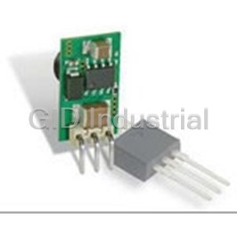
DC/DC 8-36VIN/3.3VOUT .5A SIP 7803SR-C
DC/DC 8-36VIN/3.3VOUT .5A HSIP 7803SRH-C
DC/DC 8-36VIN/5VOUT .5A SIP 7805SR-C
DC/DC 8-36VIN/5VOUT .5A HSIP 7805SRH-C
4.8 W, 15 -36 VDC VIN, SINGLE OUTPUT, 12 VDC@0.4 A DC-DC CONVERTER 7812SR-C
4.8 W, 15 -36 VDC VIN, SINGLE OUTPUT, 12 VDC@0.4 A DC-DC CONVERTER 7812SRH-C


Request a Quote

The quote request has been received

Close

Facing challenges or have inquiries? Feel free to contact us!
Call Us +1-469-283-2440
What they say about us
FANTASTIC RESOURCE
One of our top priorities is maintaining our business with precision, and we are constantly looking for affiliates that can help us achieve our goal. With the aid of GID Industrial, our obsolete product management has never been more efficient. They have been a great resource to our company, and have quickly become a go-to supplier on our list!
Bucher Emhart Glass
EXCELLENT SERVICE
With our strict fundamentals and high expectations, we were surprised when we came across GID Industrial and their competitive pricing. When we approached them with our issue, they were incredibly confident in being able to provide us with a seamless solution at the best price for us. GID Industrial quickly understood our needs and provided us with excellent service, as well as fully tested product to ensure what we received would be the right fit for our company.
Fuji
HARD TO FIND A BETTER PROVIDER
Our company provides services to aid in the manufacture of technological products, such as semiconductors and flat panel displays, and often searching for distributors of obsolete product we require can waste time and money. Finding GID Industrial proved to be a great asset to our company, with cost effective solutions and superior knowledge on all of their materials, it’d be hard to find a better provider of obsolete or hard to find products.
Applied Materials
CONSISTENTLY DELIVERS QUALITY SOLUTIONS
Over the years, the equipment used in our company becomes discontinued, but they’re still of great use to us and our customers. Once these products are no longer available through the manufacturer, finding a reliable, quick supplier is a necessity, and luckily for us, GID Industrial has provided the most trustworthy, quality solutions to our obsolete component needs.
Nidec Vamco
TERRIFIC RESOURCE
This company has been a terrific help to us (I work for Trican Well Service) in sourcing the Micron Ram Memory we needed for our Siemens computers. Great service! And great pricing! I know when the product is shipping and when it will arrive, all the way through the ordering process.
Trican Well Service
GO TO SOURCE
When I can't find an obsolete part, I first call GID and they'll come up with my parts every time. Great customer service and follow up as well. Scott emails me from time to time to touch base and see if we're having trouble finding something.....which is often with our 25 yr old equipment.
ConAgra Foods