

 Manufacturers
MURATA POWER SOLUTIONS OKLP-X/35-W12-C

Description
Non-Isolated DC/DC Converters 35A Power Block 7-13.2Vin .8-3.6Vout
Part Number
OKLP-X/35-W12-C
Price
Request Quote
Manufacturer
MURATA POWER SOLUTIONS
Lead Time
Request Quote
Category
Capacitors » DC-DC Converter
Specifications
Manufacturer
Murata Power Solutions
Manufacturers Part #
OKLP-X/35-W12-C
Series
OKLP-X/35-W12-C
Factory Pack Quantity
200
Cooling Method
Convection
Dimensions
1.00 x 0.50 x 0.44"
Efficiency
94%
Input Voltage Nominal
12 VDC
Mechanical Style
Non-Isolated / POL
Mounting
SMD/SMT
Operating Temperature
- 20 to + 70°C
Output Amps 1
35 A
Power
82.25 W
Subcategory
DC-DC Converter
Datasheet


Extracted Text
OKLP-X/35-W12-C www.murata-ps.com 35A Power Block Non-Isolated DC-DC Converter Typical unit FEATURES PRODUCT OVERVIEW Murata Power Solutions has developed the flexibility for the power systems engineer to design High efficiency (94%,12Vin, 3.3Vout@25A) OKLP-X/35-W12-C, part of a new series of “Power the power train using digital or analog controllers; Power Block (35A, 7-13Vin, 0.8-3.6Vout, SMT) Block” products to address the growing require- however, the maximum benefits are achieved when Small footprint (1" [25.4] x 0.5" [12.7] x ments for increased current/power densities coupled with ZMDI’s ZSPM1035 single-phase digi- 0.44" [11.1]) while providing maximum flexibility for power tal PWM IC controller family. The OKLP-X/35-W12 system architectures. The OKLP-X/35-W12-C has series will deliver a high efficiency, thermally stable, No minimum load required incorporated all of the power handling components high performance & cost effective solution for high Low Output Ripple required for a 35A PoL design providing maximum power/current density system requirements. -40°C to +85°C operating temperature Strong Thermal Performance Fast transient response Accurate DCR, ±5% tolerance High power density (384W/in³) in a compact footprint (1.0in. x 0.5in.) Accurate temperature sense +7V Linear Regulator Voltage Detector VIN PWM VOUT Output Filter GND GND Thermal Sensor TEMP +CS -CS Figure 1. Block Diagram For full details go to www.murata-ps.com/rohs (pending) www.murata-ps.com/support OKLP-X/35-W12-C.C01 Page 1 of 18 OKLP-X/35-W12-C 35A Power Block Non-Isolated DC-DC Converter PERFORMANCE SPECIFICATIONS SUMMARY AND ORDERING GUIDE ➀ Output Input Dimensions Efficiency ➂ Root Model Vout Iout (Amps, Power Vin nom. Range Iin, full load Inches (mm) (Volts) max.) (Watts) (Volts) (Volts) (Amps) ➁ Min. Typ. 1 x 0.5 x 0.44 OKLP-X/35-W12-C 0.8-3.6 35 82.5 12 7-13.2 12.94 91% 94.00% (25.4 x 12.7 x 11.1) ➀ Typical at Ta = +25°C ➁ @Vin = 7V, Vout = 3.3V, Iout = 25A ➂ @Vin = 12V, Vout = 3.3V, Iout = 25A PART NUMBER STRUCTURE OK L P - X / 35 - W12 - C Okami Non-isolated PoL RoHS Hazardous Substance Compliance C = RoHS-6 (does not claim EU RoHS exemption Surface Mount Power Block Input Voltage Range 7-13.2Vdc Output Voltage Range Maximum Rated Output 0.8-3.6Vdc Current in Amps ZMDI has an optimized digital controller for use with the OKLP-X/35-W12-C. See page 17 for ordering/additional information. www.murata-ps.com/support OKLP-X/35-W12-C.C01 Page 2 of 18 OKLP-X/35-W12-C 35A Power Block Non-Isolated DC-DC Converter 1. Input Requirements 1.1. Voltage: Parameter Notes Min Nom Max Units Vin (Pin 6): Operating 7 12 13.2 V Absolute max 15.0 +7V (Pin 5): Operating 6.7 7 7.5 Under-voltage lockout, rising 5.9 V Under-voltage lockout, falling 4.75 Hysteresis 0.75 1.0 PWM (Pin 3): High 2.5 5.5 V Low 1, 2 0.8 Tri-state current -10 10 µA 1. Sourcing or sinking current to/from PWM (Pin 3) within the specified range will result in both high and low-side MOSFETs to be held off by the gate-driver circuitry. 2. Before the PWM signal is applied to pin #3 (PWM), ensure that +7V is applied to the gate driver IC supply (pin 5). Other- wise, permanent damage may result to the unit. 1.2. Current: Parameter Notes Min Nom Max Units Vin = 7V, Vout = 3.3V, Iout = 25A 12.94 A Vin = 7V, Vout = 1.8V, Iout = 30A 8.77 A Vin = 12V, Vout = 1.8V, Iout = 30A 5.1 A +7V (Pin 5) (Switching at 500 KHz) 40 mA 2. Output Requirements 2.1. Voltage: Parameter Notes Min Nom Max Units Operating Range 0.8 3.6 V 2.2. Current per Phase: Parameter Notes Min Nom Max Units Operating Range 1.0Vout 1 0 35 A 1.8Vout 1 0 30 A 3.3Vout 1 0 25 A 1. 7V to 12V input, switching at 500KHz. www.murata-ps.com/support OKLP-X/35-W12-C.C01 Page 3 of 18 OKLP-X/35-W12-C 35A Power Block Non-Isolated DC-DC Converter 2.3. Power/Efficiency Parameter Notes Min Nom Max Units Output Power 82.5 W Vout = 3.3V, Iout = 25A, Vin = 12V 91 94 % Vout = 3.3V, Iout = 25A, Vin = 7V 92 95 % Vout = 1.8V, Iout = 30A, Vin = 12V 89 92 % Efficiency: 1, 2 Vout = 1.8V, Iout = 30A, Vin = 7V 88 92 % Vout = 1V, Iout = 35A, Vin = 12V 86 88.8 % Vout = 1V, Iout = 35A, Vin = 7V 86 90 % 1. 35A output, 7V to 12V input, switching at 400KHz, with 200 LFM at 55C 2. Gate drive and controller losses are included. For the purpose of this calculation, controller loss is assumed to be 0.2W. 2.4. Capacitor Parameter Notes Min Nom Max Units Input Capacitance 1, 3 52 µF Output Capacitance 2, 3 20.1 µF 1. 3 X 10µf, 25V, X7R; 1 X 22µf, 25V, X5R; 2 X 0.68µf, 25V, X8L 2. 2x 10µF/0805/6.3V/X7R + 1x 0402/0.1µF/16V/X7R. 3. Additional input and output capacitors are to be added externally as part of the buck regulator design. 2.5. Resistor Parameter Notes Min Nom Max Units Output-to-GND Resistor 1 200 Ohm 1. 0603 resistor. 2.6. Inductor Parameter Notes Min Nom Max Units Inductance 337 375 413 nH DCR (25C) 1 0.51 0.54 0.57 mOhm Isat (125C) 40 A 1. See Block Diagram for DCR sense requirements. 3. Temperature Sense Parameter Notes Min Nom Max Units Bias current sourced from controller (into Pin 4) 495 uA Voltage at 25C (Pin 4) 1.345 1.35 1.36 V Temperature coefficient (0 to 130 C) -4.4 mV / C www.murata-ps.com/support OKLP-X/35-W12-C.C01 Page 4 of 18 OKLP-X/35-W12-C 35A Power Block Non-Isolated DC-DC Converter 4. Mechanical 4.1. General Single-board, designed for machine pick-N-place. Footprint is 0.5" x 1.0". Maximum height is 0.48". Parameter Notes Nom Units Dimensions 1 x 0.5 x 0.44 inches 25.4 x 12.7 x 11.1 mm Weight 0.239 ounces 6.8 grams 4.2. Pinout Pin # Name Function 1, 10 Vout Output voltage 2, 9, 11 GND Ground for both input and output 3 PWM 3.3V compliant PWM signal to the gate driver 4 Temperature From temperature sense device on the power block for temperature sensing. 5 +7V Input voltage for gate driver 6 Vin Input voltage for the MOSFET 7 -Cs Negative DCR sense 8 +Cs Positive DCR sense 4.3. Mechanical Specifications 25.9 1.02 5.00 1.6 .197 .06 1 2 3 4 5 5.1 .20 10.16 13.2 11 .400 .52 10 9 8 7 6 2.74 1.96 11x .108 11X .077 3.0 20.00 .12 .787 RECOMMENDED FOOTPRINT (VIEWED THROUGH POWER BLOCK) Figure 2. Recommended Footprint www.murata-ps.com/support OKLP-X/35-W12-C.C01 Page 5 of 18 OKLP-X/35-W12-C 35A Power Block Non-Isolated DC-DC Converter 0.025 X 45° 25.4 11.1 (PIN #1 1.00 0.44 INDICATOR) 6.00 0.236 12.7 .50 0.25 8.1±2.3 0.010 0.32±.09 MIN ALL PINS COPLANAR 2.7 20.00 WITHIN .004" 0.11 0.787 5.00 0.197 10 9 8 7 6 10.16 1.60 11 0.400 10x 0.063 1 2 3 4 5 1.2 0.05 PIN #1 2.29 INPUT/OUTPUT CONNECTIONS 10x 0.090 Pin Function DIMENSIONS ARE IN INCHES [mm] 1 Vout TOLERANCES: 2 Gnd 2 PLACE .02 ANGLES: 1 3 PWM 3 PLACE .010 Temp 4 5 +7v COMPONENTS SHOWN ARE FOR REFERENCE ONLY 6 Vin MATERIAL: 7 -CS PINS: COPPER ALLOY 8 +CS THIRD ANGLE PROJECTION Gnd 9 FINISH: (ALL PINS) 10 Vout GOLD (5u"MIN) OVER NICKEL (50u" MIN) 11 Gnd Figure 3. Mechanical Dimensions www.murata-ps.com/support OKLP-X/35-W12-C.C01 Page 6 of 18 OKLP-X/35-W12-C 35A Power Block Non-Isolated DC-DC Converter Tape and Reel Information (MSL Rating 2) TAPE AND REEL 7770234 SHIPPING KIT TAPE AND REEL WITH MSL2 PACKAGING (NOT SHOWN) 200 UNITS PER REEL C L .025 X 45° (PIN #1 330.2 INDICATOR) 13.00 8.1±2.3 .32±.09 PICKUP POINT 6.00 .236 FEED (UNWIND) DIRECTION 4.00 2.00 .157 ROUND HOLES (SPROCKET .079 REF HOLES) ALONG THIS EDGE 20.20 .795 40.40 44.00 1.591 1.732 PICKUP NOZZLE LOCATION* 24.00 (6.3mm DIA) .945 OBLONG HOLES (SPROCKET PITCH HOLES) ALONG THIS EDGE COVER TAPE Figure 4. Tape and Reel www.murata-ps.com/support OKLP-X/35-W12-C.C01 Page 7 of 18 OKLP-X/35-W12-C 35A Power Block Non-Isolated DC-DC Converter 5. Block Diagram +7V Linear Regulator Voltage Detector VIN PWM VOUT Output Filter GND GND Thermal Sensor TEMP +CS -CS Figure 5. Block Diagram For DCR sensing, there is a 2.37KΩ resistor on the power block (between CS+ and output inductor as shown) to work with an external 0.22µf capacitor (not supplied with the power block). The external C shown as across CS+ and CS- pins should be installed on the PCB near the controller. The R value in the RC network is the inductor DCR, used in the relation L/(DCR+PCB trace)=RC. (PCB trace equal 0.1mΩ.) 6. Miscellaneous 6.1. Environmental Parameter Notes Min Nom Max Units Temperature, Operating -40 - 85 °C Temperature, Storage -40 - 125 °C Available airflow (along either long or short side) 200 - - LFM Altitude, Operating 1 -500 - 10,000 Feet Relative Humidity, Operating, Non-Condensing 10 - 90 % MSL Rating 2 1. Derate operating temperature 1°C per 1000 Feet of altitude above sea-level. www.murata-ps.com/support OKLP-X/35-W12-C.C01 Page 8 of 18 OKLP-X/35-W12-C 35A Power Block Non-Isolated DC-DC Converter 6.2. Reliability Parameter Notes Min Nom Max Units Calculated MTBF 1 3.0 - - MHrs Service Life 2 7 - - Years 1. Calculated according to Bellcore or Telcordia TR-NTW-000332 at 40C full-load. 2. Calculated at 30°C. 6.3. Parallel Operation 2 or more units will be operated in parallel. Current sharing function will be performed by the external PWM controller. 6.4. SMT Reflow Soldering Guidelines The surface-mount reflow solder profile shown below is suitable for SAC305 type lead-free solders. This graph should be used only as a guideline. Many other factors influence the success of SMT reflow soldering. Since your production environment may differ, please thoroughly review these guidelines with your process engineers. www.murata-ps.com/support OKLP-X/35-W12-C.C01 Page 9 of 18 OKLP-X/35-W12-C 35A Power Block Non-Isolated DC-DC Converter TYPICAL PERFORMANCE DATA Efficiency vs. Line Voltage and Load Current @ +25˚C. (Vout = 1.0V) Efficiency vs. Line Voltage and Load Current @ +25˚C. (Vout = 1.8V) 100 100 95 95 90 90 VIN = 7V VIN = 7V VIN = 10V 85 85 VIN = 10V VIN = 12V VIN = 12V 80 80 75 75 70 70 65 65 60 60 55 55 50 50 0 5 10 15 20 25 30 35 0 5 10 15 20 25 30 35 Load Current (Amps) Load Current (Amps) Efficiency vs. Line Voltage and Load Current @ +25˚C. (Vout = 3.3V) Maximum Current Temperature derating at Sea Level (Vout = 1V; Vin=7-13.2V) 100 40 95 35 90 VIN = 7V Still Air 30 VIN = 10V 85 0.5 m/s (100 LFM) VIN = 12V 25 1.0 m/s (200 LFM) 80 20 75 15 70 10 65 60 5 55 0 -5 0 5 10 15 20 25 30 35 40 45 50 55 60 65 70 75 80 85 90 50 Ambient Temperature (°C) 0 5 10 15 20 25 30 35 Load Current (Amps) Maximum Current Temperature derating at Sea Level (Vout = 1.8V; Vin=7-13.2V) Maximum Current Temperature derating at Sea Level (Vout = 3.3V; Vin=7-13.2V) 40 30 35 25 30 Still Air 20 0.5 m/s (100 LFM) Still Air 25 0.5 m/s (100 LFM) 20 15 1.0 m/s (200 LFM) 15 10 10 5 5 0 0 -5 0 5 10 15 20 25 30 35 40 45 50 55 60 65 70 75 80 85 90 -5 0 5 10 15 20 25 30 35 40 45 50 55 60 65 70 75 80 85 90 Ambient Temperature (°C) Ambient Temperature (°C) www.murata-ps.com/support OKLP-X/35-W12-C.C01 Page 10 of 18 Output Current (Amps) Efficiency (%) Efficiency (%) Output Current (Amps) Output Current (Amps) Efficiency (%) OKLP-X/35-W12-C 35A Power Block Non-Isolated DC-DC Converter TYPICAL PERFORMANCE DATA Efficiency vs. Load Current (Vo=1V, Vin=12Vin, 25°C, 0LFM) Efficiency vs. Load Current (Vo=1V, Vin=12Vin, 25°C, 100LFM) 100 100 95 95 90 90 85 85 80 80 400KHZ 400KHZ 75 75 500KHZ 500KHZ 70 70 600KHZ 600KHZ 65 65 60 60 0 5 10 15 20 25 30 35 0 5 10 15 20 25 30 35 Load Current (Amps) Load Current (Amps) Efficiency vs. Load Current (Vo=1V, Vin=12Vin, 25°C, 200LFM) Efficiency vs. Load Current (Vo=1.8V, Vin=12Vin, 25°C, 0LFM) 100 100 95 95 90 90 85 80 85 400KHZ 400KHZ 75 80 500KHZ 500KHZ 70 600KHZ 600KHZ 75 65 60 70 0 5 10 15 20 25 30 35 0 5 10 15 20 25 30 Load Current (Amps) Load Current (Amps) Efficiency vs. Load Current (Vo=1.8V, Vin=12Vin, 25°C, 100LFM) Efficiency vs. Load Current (Vo=1.8V, Vin=12Vin, 25°C, 200LFM) 100 100 95 95 90 90 85 85 400KHZ 400KHZ 80 80 500KHZ 500KHZ 600KHZ 600KHZ 75 75 70 70 0 5 10 15 20 25 30 0 5 10 15 20 25 30 Load Current (Amps) Load Current (Amps) www.murata-ps.com/support OKLP-X/35-W12-C.C01 Page 11 of 18 Efficiency (%) Efficiency (%) Efficiency (%) Efficiency (%) Efficiency (%) Efficiency (%) OKLP-X/35-W12-C 35A Power Block Non-Isolated DC-DC Converter TYPICAL PERFORMANCE DATA Efficiency vs. Load Current (Vo=3.3V, Vin=12Vin, 25°C, 0LFM) Efficiency vs. Load Current (Vo=3.3V, Vin=12Vin, 25°C, 100LFM) 100 100 95 95 90 90 85 85 400KHZ 400KHZ 80 80 500KHZ 500KHZ 600KHZ 600KHZ 75 75 70 70 0 5 10 15 20 25 0 5 10 15 20 25 Load Current (Amps) Load Current (Amps) Efficiency vs. Load Current (Vo=3.3V, Vin=12Vin, 25°C, 200LFM) 100 95 90 85 400KHZ 80 500KHZ 600KHZ 75 70 0 5 10 15 20 25 Load Current (Amps) www.murata-ps.com/support OKLP-X/35-W12-C.C01 Page 12 of 18 Efficiency (%) Efficiency (%) Efficiency (%) OKLP-X/35-W12-C 35A Power Block Non-Isolated DC-DC Converter TECHNICAL NOTES Overview * The “Power Stage” of a Non-isolated PoL: Murata Power Solutions has developed the OKLP-X/35-W12-C, part of a • Does “the heavy lifting”—FETs, output inductor, gate drive circuitry new series of “Power Block” products to address the growing requirements • Synchronous buck converter topology (evaluated at 400-600 KHz) for increased current/power densities while providing maximum flexibility • Requires external parts for a complete POL solution (PWM, etc.) for power system architectures. The OKLP-X/35-W12-C has incorporated all • Can accommodate analog or digital controllers of the power handling components required for a 35A PoL design providing In order to implement a complete POL solution, external circuitry must be maximum flexibility for the power systems engineer to design the power added in the form of a PWM controller, gate drive voltage, as well as input train using digital or analog controllers; however, the maximum benefits and output capacitors. The Power Blocks are designed to accommodate are achieved when coupled with ZMDI’s ZSPM1035 single-phase digital either analog or digital PWM controllers, affording customers a wide range PWM IC controller family. The OKLP-X/35-W12 series will deliver a higher of performance features and functionality, according to their needs. For efficiency, thermally stable, high performance & cost effective solution for dense PCB circuit implementations, the PWM controller can be mounted on high power/current density system requirements. the underside the PCB, resulting in a very dense PCB layout. Compelling advantages 35A Power Block: Murata Power Solutions’ Power Blocks offer compelling advantages to users seeking flexibility and ease-of-use, including the following: +7V Linear • High efficiency, high power density (384 W/in³) in a compact footprint Regulator (1.0in. x 0.5in.) • Accurate DCR, ±5 % tolerance Voltage Detector • Accurate temperature sense VIN • Ease of use; Simpler pcb layout; Noise/EMI contained within Power Block • PMBus option (depending on PWM IC used) • Current sharing options (depending on PWM IC used) PWM VOUT Output • Cost between down-solutions and integrated PoL modules Filter • PCB area/BOM reduction vs. fully discrete solutions GND GND • Compatible with multiple PWM IC suppliers (e.g., IR, Linear Tech, Powervation, TI, ZMDI) Thermal Sensor TEMP The ease-of-use aspect of the Power Blocks enables users to reduce the design cycle and improve the time-to-market. The Power Blocks are a high +CS reliability solution with a calculated MTBF of 3 MH (min.) and Service Life -CS of 6 years. Controlled variances and tight control over the inductor DCR, for example, ±5 % tolerance vs. ±10%, typically, enables more accurate current sense. In all these variables and features, “Knowing what you get” Figure 6. 35A Power Block is important in realizing a successful and reliable design. * 0.22µf external capacitor must be used for accurate current sense The OKLP-X/35 Power Block can be used with most analog or digital PWM controller IC. By simplifying the design task and providing for a high-density layout, including a reduced BOM (e.g., output capacitance), depending on transient performance vs. output capacitance, the OKLP-X/35 Power Block enables a robust design, reduced total cost of ownership and higher energy efficiency across all output load conditions. Basic informa- INPUT/OUTPUT CONNECTIONS tion, including efficiency, thermal derating, etc., for the Power Block alone, Pin # Name Function not including controller losses, has been characterized. 1, 10 Vout Output voltage Contact Murata Power Solutions for further information. 2, 9, 11 GND Ground for both input and output 3 PWM 3.3V compliant PWM signal to the gate driver Each pin of the Power Block and related functional information for the 4 Temp From temperature sense device on the power block for temperature sensing. controller (PWM) are described. 5 +7V Input voltage for gate driver Discussion 6 Vin Input voltage for the MOSFET The OKLP-X/35 Power Block is not a completely integrated point-of-load 7 -Cs Negative DCR sense (PoL) solution. Power Blocks comprise the Power Stage* of a non-isolated 8 +Cs Positive DCR sense converter, integrating the power FETs, output inductor, current sense, tem- perature sense, and gate drive circuitry of a synchronous buck converter. This is the part of a PoL that performs the “heavy lifting” in the conversion process. www.murata-ps.com/support OKLP-X/35-W12-C.C01 Page 13 of 18 OKLP-X/35-W12-C 35A Power Block Non-Isolated DC-DC Converter PCB Design Guidelines • It is important to note that hole plating thickness and circumference must be used to determine the cross section when calculating the cur- Guidelines for proper conductor (surface and buried traces, vias, etc.) rent carrying capacity of vias. Hole plating thickness will be much thinner copper plating, pad sizes, trace widths, spacing, etc., can be found in IPC- than the copper weight of the printed circuit board. 2221A, “Generic Standard on Printed Circuit Board Design.” Please consult this or similar standards when designing PCB layouts for the high-current IPC-2221A Formula for Calculating Trace Width and Vias output from the OLKP Power Blocks or any high-current power supply, 0.44 0.725 I = kΔT A taking into consideration, maximum currents, temperature rise and convec- WHERE: tion and/or conduction cooling of the end-user application. I = current in amperes Powerblock Power Pins A = cross section in sq mils Placing large vias close to the power pins will improve thermal perfor- ΔT = temperature rise in °C mance. Connecting each group of power and ground vias together on all k is a derating constant such that: inner layers where possible with a copper area will improve heat dissipation. k = .048 for outer layers k = .024 for inner layers Via Construction and Sizing • Via diameter and copper plating thickness affect current carrying capacity. Input/Output Capacitor Selection • Increasing outer layer copper thickness will allow thicker via plating The required amount of input and output capacitance will be determined thickness. MPS uses 3 Oz outer layers for 1 Oz via plating. on an application by application basis. However, there are guidelines • Increased via plating thickness will prevent barrel cracking when board common to every design which can be identified and following is a very temperature changes to extremes, including reflow, resulting in improved brief overview. reliability. For instance, ceramic capacitors with very low ESR (and ESL, if pub- The following chart shows that larger diameter vias or thicker copper lished) should be selected to reduce input and output ripple voltages. These plating will improve the current carrying capacity. should be placed as close to the power supply input as practical. External ΔT input bypass “bulk” capacitance should then be determined in order to k stabilize the input voltage during large load transients and supply extra cur- A = (Diameter * PI * Plating) rent to the load during a step load change. The maximum output capacitive I = (k * (T ^ 0.44)) * (A ^ 0.725) loading specified in the datasheet should be observed. Consideration must Via wall plating thickness (oz) also be given to ripple voltage and currents and the impact on capacitor Via Diameter (mils) 1.00 0.50 0.25 lifetime and system reliability. Note that both input and output capacitors 10 1.54 A 0.93 A 0.56 A should be placed close to the load. 15 2.06 A 1.25 A 0.75 A Also, as some systems are difficult to fully characterize analytically, 20 2.54 A 1.54 A 0.93 A some empirical testing may be necessary to assure successful operation. 25 2.99 A 1.81 A 1.09 A 30 3.41 A 2.06 A 1.25 A Input Capacitor Selection 35 3.81 A 2.31 A 1.40 A Reduce Input Ripple Voltage: The first step is to reduce ripple voltage 40 4.20 A 2.54 A 1.54 A amplitude at the input of the converter. For this purpose, ceramic capacitors 50 4.94 A 2.99 A 1.81 A with very low ESR should be selected; large, bulk capacitors do not reduce 60 5.63 A 3.41 A 2.06 A ripple voltage, as the ESR of aluminum electrolytics and most tantalums are ΔT = Max temperature rise above ambient (25°C) too high to allow for effective ripple reduction. Therefore, to reduce the rms k = Derating constant (.024) current in the bulk capacitors the ripple voltage amplitude must be reduced A = Area in square mils using ceramic capacitors. From the literature, “as a general rule of thumb, I = Current in Amps keeping the peak to peak ripple amplitude below 75 mV keeps the rms For optimum performance, heavy copper (2 Oz or greater) or use of multiple currents in the bulk capacitors within acceptable limits. copper layers should be used for all power connections. “Load current, duty cycle, and switching frequency are several factors For higher currents, improved thermal performance and increased reli- which determine the magnitude of the input ripple voltage. The input ripple ability of the power converter, the following suggestions are recommended: voltage amplitude is directly proportional to the output load current. The • Multiple vias capable of carrying the current required should be used. maximum input ripple amplitude occurs at maximum output load. Also, the Two adequately sized vias per amp. is not uncommon. amplitude of the voltage ripple varies with the duty cycle of the converter. • Vias should be placed as close to power pins as permissible. For a single phase buck regulator, the duty cycle is approximately the ratio • Use of thermal reliefs for vias and power pads should be avoided. of output to input dc voltage. A single phase buck regulator reaches its maximum ripple at 50% duty cycle.” Further detail can be found in the • Unused inner layer via pads should not be removed. This annular ring literature. reduces the resistance and increases the copper area of the via. Con- necting these vias together on as many inner layers as possible using The following equation can be used to determine the amount of ceramic copper fills will also improve via performance. capacitance required to reduce the ripple voltage amplitude to acceptable levels: www.murata-ps.com/support OKLP-X/35-W12-C.C01 Page 14 of 18 OKLP-X/35-W12-C 35A Power Block Non-Isolated DC-DC Converter C = (Iout x DC X (1-DC) x 1000)/(F x Vpmax), DC=Vout/(Vin x η); The magnitude of the input current transient is calculated from the fol- MIN SW η=Efficiency lowing equation: Where Delta I =V /(V x η) x delta I , where IN OUT IN OUT F is the switching frequency in KHz SW • η is efficiency Iout is the steady state output load current • C is the minimum required ceramic input capacitance in µF ➀ MIN • ΔI is the output transient current OUT VP is the maximum allowed peak-peak ripple voltage ➁ (MAX) • ΔI is the input transient current IN Example Ceramic Calculation • V is the nominal output voltage OUT Given: • V is the nominal input voltage IN • VIN = 12 V The efficiency value η is obtained from the regulator data sheet. Use a • VOUT = 3.3 V value from the efficiency curve for the particular output voltage and the • IOUT = 10 A highest expected output current. • η = 90% Next, determine the maximum allowable voltage deviation on the • F = 333 kHz SW bulk capacitors. This is the maximum allowable dip during the peak • DC = 0.3 transient step that was calculated in step one. The smaller the voltage The minimum ceramic capacitance required to reduce the ripple voltage to deviation, the higher the required amount of bulk capacitance. 75 mVpp is calculated to be: The following equation calculates the minimum required bulk capacitance. C =(10A x 0.3 x (1-0.3) x 1000)/333 x 75mV = 84µF MIN 2 2 C = (1.21 x ΔI x L)/ΔV IN ➀ The actual capacitance of a ceramic is less than the stated nominal value at a given DC voltage. Make sure Where: the actual value is equal to or greater than the calculated value. ΔI is the change in input current in response to the output step load IN ➁ 75 mVpp is recommended Vpmax. This will yield approximately 22 mVrms of ripple voltage. transient Transients and Bulk Capacitors L is stray inductance in the host supply path and/or any series inductor ➂ ΔV is the allowable input voltage dip following the output step load transient Bulk capacitors control the voltage deviation at the input when the con- verter is responding to an output load transient. The higher the capacitance, Note that this equation is an approximation. The value it produces should the lower the deviation. Therefore, the size of the input bulk capacitor is be considered to be an absolute minimum amount. The exact value will determined by the size of the output current transient and the allowable have to be determined through experimentation depending on how well input voltage deviation. The amplitude of the input voltage deviation during regulated your host supply is. a transient is directly proportional to the load current change. If the magni- Example tude of the transient load current is doubled, the input voltage disturbance • Assume filter L = 560 nH is doubled also. • Assume allowable ΔV is 100 mV Lower input voltage means higher input currents. The input current • Assume input transient current (ΔI ) was calculated to be 2.774A IN scales directly by duty cycle. At lower input voltages the input transient 2 2 2 -9 2 C = (1.21 x ΔI x L)/ΔV = (1.21 x (2.774) x 560 x 10 )/(-.100) = 521 µF IN currents will also be higher. To comply with output voltage deviation limits, more input capacitance is required. According to the calculation, a minimum 521μF of bulk capacitance is needed. Use the nearest standard value of 560 µF. Consider a 2.5V output regulator with a 10A transient load. With a 12V input, the ideal duty cycle is 2.5/12 = 0.208. The 10 A load transient on ➂ The user needs to decide if a series filter inductor is going to be used. If using an inductor, pick a value no the output transforms to a 2.08A transient on the input. With a 3.3 V input greater than 560 nH. If not using one, use a value of 50 nH in the calculation to account for stray inductance in the host supply path and its finite bandwidth. regulator, the duty cycle is now 2.5/3.3=0.758. The 10 A load transient is Detailed discussion of the use of an input inductor is beyond the scope of these guidelines, however; if now a 7.58A input transient. This will cause a larger voltage deviation on reflected ripple is a concern, a small (560 nH or less) input inductor can be used. At lower currents, this input the lower voltage supply where the voltage limits are probably tighter. inductor can take the form of a power ferrite bead. This is an effective way to confine ripple currents to the local input bypass caps. An input inductor can reduce the reflected ripple current by an order of magnitude. During a transient, input inductance slows the current slew rate seen by During transient conditions, the use of an input inductor puts larger demands on input bulk capacitors. Take care when using input inductors as they will affect input capacitor selection. the host supply. The use of a filter inductor places more demands on the input bulk capacitors since more of the initial current demand must come Output Capacitor Selection from the input capacitors rather than the host supply. The input voltage at There are numerous factors to consider when adding external capacitors to the regulator input now sees a much higher voltage deviation. In the end, switched-mode power supplies (SMPS), including noise, startup, ESR, sta- both the input and output capacitors have to be recharged, causing higher bility, pre-bias applications, Sense inputs, On/Off (remote enable) controls peak currents to be demanded from the host supply. and other topics. Bulk input capacitance calculation example Most DC-DC applications require external bypass “bulk” capaci tors as When designing a system consisting of a single POL module, the first step part of the output load. These capacitors supply extra current during a step is to calculate the magnitude of the input transient current. This is done load change. Lower DC voltages used in newer logic devices mean that the by calculating the reflected input transient for each POL module’s output voltage margin difference between logic ZERO and logic ONE is reduced to transient. When calculating, you must determine the worst case transient hundreds or even tens of millivolts. Thus, since even modest power supply combination of all modules and proceed accordingly. www.murata-ps.com/support OKLP-X/35-W12-C.C01 Page 15 of 18 OKLP-X/35-W12-C 35A Power Block Non-Isolated DC-DC Converter noise can cause data errors by exceeding this threshold, these bypass caps protection circuit. Furthermore, each over-current trip will be followed by are necessary to reduce this DC-DC noise. further attempts by the regulator to restart. This can result in the regulator entering a perpetual cycle of over-current shutdown. In addition to the possibility of failed or delayed startup, increasing external capacitance can cause sluggish transient response, possible Data sheet tables give the maximum allowable output capacitance ringing and instability. The maximum output capacitive load specification is for each module. If external capacitance is required for stable operation, really an indication of acceptable and stable startup performance but with the minimum value will be listed in the datasheet. Recommended capaci- moderated transient response. tance is also listed in the datasheet for improved transient performance. The recommended capacitance value will meet a typical ΔV spec at a 50% Designing for Transient Performance transient load step. When designing for a load transient, the output bulk capacitors and high Detailed analysis has been performed to allow capacitor limits to be frequency bypass capacitors determine the response performance and accurately defined. By following the capacitor recommendations in the data voltage deviation of the regulator. The most important parameters are the sheet and selecting capacitors based on your actual operating conditions, a magnitude of the load transient (ΔI) and the distributed bus impedance to reliable, low-cost power system can be designed. the load. The selection of the output capacitors is determined by the allowable peak voltage deviation (ΔV). This limit should reflect the actual Additional explanation can be found at the Murata Power Solutions web requirements, and should not be specified lower than needed. page at www.murata-ps.com/data/apnotes/dcan-58.pdf, Application Note D-CAN-58, Output Capacitive Load Considerations. The distribution bus impedance seen by the load is the parameter that determines the peak voltage deviation during a fast transient. The system Power Block Performance requires a low impedance bus over all frequencies with adequate bypass The OKLP-X/35 Power Block modules have been tested using controller capacitors to achieve fast slew rates. If the impedance of the network (PWM) IC’s under various transient load conditions. Contact Murata Power that supplies the load remains below a maximum impedance, the voltage Solutions for further details. deviation due to the transient will remain within allowable voltage deviation requirements. It is simply Ohm’s Law: ΔV= ΔI x Z. Keep the magnitude of Power Block Pin Functional Descriptions Z below the maximum limit, and the transient voltage deviation will stay Pin #2, 9, 11 (Gnd) within its limits. Pin #3 (PWM): Divide ΔV by the ΔI to determine the maximum allowable impedance, This is a 3.3V logic level tri-state PWM input and 5V tolerant. “High” turns Zmax. This is the impedance limit which must be maintained by the output the control MOSFET on, and “Low” turns the synchronous MOSFET on. capacitor network for frequencies above which the regulator is effective. To “Tri-state” turns both MOSFETs off. In diode emulation mode, “Tri-state” maintain low impedance from the regulator to the load, high frequency, low activates internal diode emulation control. value ceramic capacitors must be placed very close to the load to minimize the effects of trace inductance while larger value ceramic capacitors can Pin #4 (Temperature): Temperature Measurement be placed closer to the regulator. The OKLP-X/35 includes a Thermal Sensor in the module for temperature sensing of the inductor. This element is used by the controller for tempera- Transient Design Example ture compensation, measuring the inductor temperature. This information Calculating the maximum allowable output impedance, given the following can be used to adapt the gain of the current sense path to compensate for requirements: the increase in actual DCR. • VO = 2.5 V Pin #5 (+7V): Supply to the gate driver IC (6.7V to 7.5V). This can be • Output current step from 0.8 A to 12.5 A (ΔI = 11.7 A) supplied via another +5V power rail, or a linear regulator or an LDO (e.g., • Maximum allowable voltage deviation (ΔV) is 100 mV LM317 or LP2992). • 20 A/μsec slew rate. ΔV/ΔI = Maximum impedance Pin #6 (Vin): ΔV/ΔI = 100 mV/11.7 A = 8.55 mΩ Input supply pin, with a range of 7 – 13.2Vin (see 1.1). Pin #8 (+Cs), Positive DCR (current) sense and Pin #7 (-Cs), Negative DCR Selecting four 330 μF capacitors with an ESR of 25 mΩ would provide (current) sense: For additional information, please reference the relevant an effective ESR of 6.25 mΩ and 1320 μF of total capacitance. Using these applications notes (www.zmdi.com/zspm1000) for the specific controller capacitors, the actual amplitude of the transient deviation would be about (PWM) IC to be used. Contact Murata Power Solutions for further infor- ±73 mV (11.7 A × 6.25 mΩ). By maintaining the low impedance over the mation. A brief description of using current sense with the Power Block complete frequency range, any high slew rate transient will be achieved. follows. Absolute Maximum Capacitor Limits Current Sensing All regulators have an absolute maximum capacitance limit. MPS DC-DC Many controller (PWM) IC’s implement average current sensing to provide converter modules incorporate output short-circuit protection. During accurate current information over the switching period. A generated startup, the regulator must charge the output capacitance in order to raise schematic of the required current sensing circuitry is shown in figure 7 the output voltage to its set-point and this current flow is in addition to any for the widely used DCR current-sensing method, which uses the parasitic load current that may be drawn by the application circuit. If there is too resistance of the inductor to acquire the current information. The principle much output capacitance, the current demanded from the regulator trips its is based on a matched time-constant (i.e., RC=L/R (DCR) between the over-current www.murata-ps.com/support OKLP-X/35-W12-C.C01 Page 16 of 18 OKLP-X/35-W12-C 35A Power Block Non-Isolated DC-DC Converter inductor and the low-pass filter built from the 2.15KΩ resistor and an exter- +7V Linear nal capacitor (not supplied with the OKLP-X/35 Power Block) across +Cs Regulator and –Cs (220µf), where the inductor L and DCR (+5%) values are used. Pin #1, 10 (Vout): Output voltage supplied to the load. Note: There is Voltage minimal input/output capacitance incorporated in the Power Block. Detector Approximately 600μf output capacitance is “typical” at 35A output current VIN level, depending on the application. Refer to 2.4. Capacitor (OKLP-X/35 datasheet). The user needs to determine the appropriate amount of external capacitance for energy storage, ripple voltage requirements, etc. PWM VOUT Output Filter Power Block Design Process GND GND The design process begins with selecting a PWM controller for use with the OKLP-X/35-W12 Power Block. As each controller (PWM) IC differs in Thermal Sensor TEMP configuration and performance, the user needs to ensure that adequate technical support is available from the supplier of choice (e.g., datasheets, +CS application notes and configuration tools). For details concerning usage -CS with a Power Block (i.e., the “power stage”) to implement a point-of- load solution, including regulation, transient performance, protection and sequencing, please consult the supplier’s web page. Contact Murata-PS Figure 7. Inductor Current Sensing Using the DCR Method Technical Support (www.murata-ps.com/support), as well as the websites below, for further information. www.zmdi.com/Murata_Power_Block www.powervation.com/products/single-phase-controllers DEDICATED CONTROLLER P/N TO SUPPORT MURATA POWER BLOCKS ZMDI P/N Murata Power Solutions P/N Iout Vout Voltage Divider Setting Output Capacitor Release Date ZSPM1035AA1R 0.35V-3.6V Programmable 4 fixed different ranges ZSPM1035CA1R OKLP-X/35-W12-C 35A 0.6V-1.2V No voltage divider December 2013 4 fixed different ranges selectable by pin-strap option ZSPM1035DA1R 1.2V-3.4V With voltage divider www.murata-ps.com/support OKLP-X/35-W12-C.C01 Page 17 of 18 OKLP-X/35-W12-C 35A Power Block Non-Isolated DC-DC Converter 7 7 3 Figure 8. Typical OKLP-X/35-W12 - controller implementation This product is subject to the following operating requirements Murata Power Solutions, Inc. and the Life and Safety Critical Application Sales Policy: 11 Cabot Boulevard, Mansfield, MA 02048-1151 U.S.A. Refer to: http://www.murata-ps.com/requirements/ ISO 9001 and 14001 REGISTERED Murata Power Solutions, Inc. makes no representation that the use of its products in the circuits described herein, or the use of other technical information contained herein, will not infringe upon existing or future patent rights. The descriptions contained herein do not imply the granting of licenses to make, use, or sell equipment constructed in accordance therewith. Specifications are subject to change without notice. © 2017 Murata Power Solutions, Inc. www.murata-ps.com/support OKLP-X/35-W12-C.C01 Page 18 of 18
Frequently asked questions
How does Electronics Finder differ from its competitors?

Is there a warranty for the OKLP-X/35-W12-C?
Which carrier will Electronics Finder use to ship my parts?
Can I buy parts from Electronics Finder if I am outside the USA?
Which payment methods does Electronics Finder accept?
Why buy from GID?

Quality
We are industry veterans who take pride in our work

Protection
Avoid the dangers of risky trading in the gray market

Access
Our network of suppliers is ready and at your disposal

Savings
Maintain legacy systems to prevent costly downtime

Speed
Time is of the essence, and we are respectful of yours
Related Products
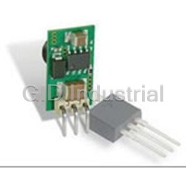
DC/DC 8-36VIN/3.3VOUT .5A SIP 7803SR-C
DC/DC 8-36VIN/3.3VOUT .5A HSIP 7803SRH-C
DC/DC 8-36VIN/5VOUT .5A SIP 7805SR-C
DC/DC 8-36VIN/5VOUT .5A HSIP 7805SRH-C
4.8 W, 15 -36 VDC VIN, SINGLE OUTPUT, 12 VDC@0.4 A DC-DC CONVERTER 7812SR-C
4.8 W, 15 -36 VDC VIN, SINGLE OUTPUT, 12 VDC@0.4 A DC-DC CONVERTER 7812SRH-C


Request a Quote

The quote request has been received

Close

Facing challenges or have inquiries? Feel free to contact us!
Call Us +1-469-283-2440
What they say about us
FANTASTIC RESOURCE
One of our top priorities is maintaining our business with precision, and we are constantly looking for affiliates that can help us achieve our goal. With the aid of GID Industrial, our obsolete product management has never been more efficient. They have been a great resource to our company, and have quickly become a go-to supplier on our list!
Bucher Emhart Glass
EXCELLENT SERVICE
With our strict fundamentals and high expectations, we were surprised when we came across GID Industrial and their competitive pricing. When we approached them with our issue, they were incredibly confident in being able to provide us with a seamless solution at the best price for us. GID Industrial quickly understood our needs and provided us with excellent service, as well as fully tested product to ensure what we received would be the right fit for our company.
Fuji
HARD TO FIND A BETTER PROVIDER
Our company provides services to aid in the manufacture of technological products, such as semiconductors and flat panel displays, and often searching for distributors of obsolete product we require can waste time and money. Finding GID Industrial proved to be a great asset to our company, with cost effective solutions and superior knowledge on all of their materials, it’d be hard to find a better provider of obsolete or hard to find products.
Applied Materials
CONSISTENTLY DELIVERS QUALITY SOLUTIONS
Over the years, the equipment used in our company becomes discontinued, but they’re still of great use to us and our customers. Once these products are no longer available through the manufacturer, finding a reliable, quick supplier is a necessity, and luckily for us, GID Industrial has provided the most trustworthy, quality solutions to our obsolete component needs.
Nidec Vamco
TERRIFIC RESOURCE
This company has been a terrific help to us (I work for Trican Well Service) in sourcing the Micron Ram Memory we needed for our Siemens computers. Great service! And great pricing! I know when the product is shipping and when it will arrive, all the way through the ordering process.
Trican Well Service
GO TO SOURCE
When I can't find an obsolete part, I first call GID and they'll come up with my parts every time. Great customer service and follow up as well. Scott emails me from time to time to touch base and see if we're having trouble finding something.....which is often with our 25 yr old equipment.
ConAgra Foods