

 Manufacturers
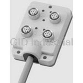
OMRON AUTOMATION K32DICN

Description
Cable Assembly Flat Ribbon 3m IDC 8 POS SKT IDT
K32DICN
Part Number
K32DICN
Price
Request Quote
Manufacturer
OMRON AUTOMATION
Lead Time
Request Quote
Category
Wire and Cables » Cable Assembly Flat/Ribbon
Specifications
Manufacturer
Omron Automation
Manufacturers Part #
K32DICN
Lead Time
4 Week Lead Time
Industry Aliases
K32-DICN
Sub-Category
Flat / Ribbon Cable Assemblies
Factory Pack Quantity
1
Datasheet

Extracted Text
Linear Sensor Indicator
K3HB-S
CSM_K3HB-S_DS_E_10_2
Linear Sensor Indicator for High-speed, High-
precision Measurement and Discrimination
Easy recognition of judgement result s using color display that can be
switched between red and green. *
Equipped with a position meter that represents measured amounts and
relative positions.
Develop a variety of measurement and discrimination applications us-
ing external event inputs.
Series expanded to include DeviceNet models.
Short body with depth of only 95 mm (from behind the front panel), or
97 mm for DeviceNet models.
UL certification approval (C ertification Mark License).
CE Marking conformance by third party assessment body.
Water-resistant enclosure conforms to NEMA 4X (equivalent to IP66).
*Visual confirmation of judgement results is not supported on models that do not
have an output or models that do not support DeviceNet.
You can change the display color by setting it, but you cannot switch it based on
the judgement results. For the most recent information on models that have been certified for
safety standards, refer to your OMRON website.
Refer to Safety Precautions for All Digital Panel
Meters.
Model Number Structure
■ Model Number Legend
Base Units and Optional Boards can be ordered individually or as sets.
Base Units Base Units with Optional Boards
K3HB-S@ K3HB-S@-@@@
12 34 5
1 5
2. Sensor Power Supply/Output Type Code
1. Input Sensor Code
None: None
SD: DC Process input
CPA: Relay output (PASS: SPDT) + Sensor power supply
(12 VDC +/10%, 80 mA) (See note 1.)
5. Supply Voltage
L1A: Linear current output (0 to 20 or 4 to 20 mA DC) + Sensor power supply
100-240 VAC: 100 to 240 VAC (12 VDC +/10%, 80 mA) (See note 2.)
L2A: Linear voltage output (0 to 5, 1 to 5, or 0 to 10 VDC) + Sensor power
24 VAC/VDC: 24 VAC/VDC
supply (12 VDC +/10%, 80 mA) (See note 2.)
A: Sensor power supply (12 VDC +/10%, 80 mA)
FLK1A: Communications (RS-232C) + Sensor power supply
(12 VDC +/10%, 80 mA) (See note 2.)
FLK3A: Communications (RS-485) + Sensor power supply
(12 VDC +/10%, 80 mA) (See note 2.)
Note: 1. CPA can be combined with relay outputs only.
2. Only one of the following can be used by each Digital Indicator: RS-
232C/RS-485 communications, a linear output, or DeviceNet
communications.
Optional Board
3. Relay/Transistor Output Type Code
Sensor Power Supply/Output Boards
None: None
C1: Relay contact (H/L: SPDT each)
K33-@
C2: Relay contact (HH/H/LL/L: SPST-NO each)
2
T1: Transistor (NPN open collector: HH/H/PASS/L/LL)
T2: Transistor (PNP open collector: HH/H/PASS/L/LL)
Relay/Transistor Output Boards
BCD: BCD output + transistor output (NPN open collector: HH/H/PASS/L/
LL)
K34-@
DRT: DeviceNet (See note 2.)
3
A Special BCD Output Cable (sold separately) is required.
4. Event Input Type Code
Event Input Boards
None: None
1: 5 inputs (M3 terminal blocks), NPN open collector
K35-@
2: 8 inputs (10-pin MIL connector), NPN open collector
4
3: 5 inputs (M3 terminal blocks), PNP open collector
4: 8 inputs (10-pin MIL connector), PNP open collector
Note: The following combinations are not possible.
Communications (FLK@A) + DeviceNet (DRT)
Communications (FLK@A) + BCD output (BCD)
Linear current/voltage (L@A) + DeviceNet (DRT)
1
K3HB-S
Accessories (Sold Separately)
K32-DICN: Special Cable (for event inputs, with 8-pin connector)
K32-BCD: Special BCD Output Cable
Watertight Cover Rubber Packing
Model
Model
Y92A-49N
K32-P1
Note: Rubber packing is provided with the Controller.
Specifications
■ Ratings
Power supply voltage
100 to 240 VAC (50/60 Hz), 24 VAC/VDC, DeviceNet power supply: 24 VDC
Allowable power supply voltage range
85% to 110% of the rated power supply voltage, DeviceNet power supply: 11 to 25 VDC
Power consumption 100 to 240 V: 18 VA max. (max. load)
(See note 1.) 24 VAC/DC: 11 VA/7 W max. (max. load)
Current consumption DeviceNet power supply: 50 mA max. (24 VDC)
Input DC voltage/current
A/D conversion method Sequential comparison system
External power supply 12 VDC ±10%, 80 mA (models with external power supply only)
Event inputs Timing input NPN open collector or no-voltage contact signal
(See note 2.)
ON residual voltage: 3 V max.
ON current at 0 : 17 mA max.
Max. applied voltage: 30 VDC max.
OFF leakage current: 1.5 mA max.
Startup compensa- NPN open collector or no-voltage contact signal
tion timer input
ON residual voltage: 2 V max.
ON current at 0 : 4 mA max.
Hold input
Max. applied voltage: 30 VDC max.
Reset input
OFF leakage current: 0.1 mA max.
Forced-zero input
Bank input
Output ratings (de- Relay output 250 VAC, 30 VDC, 5 A (resistive load)
pends on the model)
Mechanical life expectancy: 5,000,000 operations, Electrical life expectancy: 100,000 operations
Transistor output Maximum load voltage: 24 VDC, Maximum load current: 50 mA, Leakage current: 100 A max.
Linear output Linear output 0 to 20 mA DC, 4 to 20 mA DC:
Load: 500 max, Resolution: Approx. 10,000, Output error: ±0.5% FS
Linear output 0 to 5 VDC, 1 to 5 VDC, 0 to 10 VDC:
Load: 5 k max, Resolution: Approx. 10,000, Output error: ±0.5% FS
(1 V or less: ±0.15 V; no output for 0 V or less)
Display method Negative LCD (backlit LED) display
7-segment digital display (Character height: PV: 14.2 mm (green/red); SV: 4.9 mm (green)
Main functions Scaling function, 2-input calculation function, measurement operation selection, averaging, previous average value
comparison, forced-zero, zero-limit, output hysteresis, output OFF delay, output test, teaching, display value selection,
display color selection, key protection, bank selection, display refresh period, maximum/minimum hold, reset
Ambient operating temperature 10 to 55C (with no icing or condensation)
Ambient operating humidity 25% to 85%
Storage temperature 25 to 65C (with no icing or condensation)
Altitude 2,000 m max.
Accessories Watertight packing, 2 fixtures, terminal cover, unit stickers, instruction manual. DeviceNet models also include a De-
viceNet connector (Hirose HR31-5.08P-5SC(01)) and crimp terminals (Hirose HR31-SC-121) (See note 3.)
Note: 1. DC power supply models require a control power supply capacity of approximately 1 A per Unit when power is turned ON. Particular
attention is required when using two or more DC power supply models. The OMRON S8VS-series DC Power Supply Unit is recommend-
ed.
2. PNP input types are also available.
3. For K3HB-series DeviceNet models, use only the DeviceNet Connector included with the product. The crimp terminals provided are for
Thin Cables.
2
K3HB-S
■ Characteristics
Display range 19,999 to 99,999
Sampling period One input: 0.5 ms; Two inputs: 1.0 ms
Comparative out- One input OFF to ON: 1 ms max., ON to OFF: 1.5 ms max.
put response (The time until the comparative output is output when there is a forced sudden change in the input signal from 15% to 95%
times (transistor or 95% to 15%.)
outputs)
Two inputs OFF to ON: 2 ms max., ON to OFF: 2.5 ms max.
(The time until the comparative output is output when there is a forced sudden change in the input signal from 15% to 95%
or 95% to 15%.)
Linear output re- One input 51 ms max.
sponse time (The time until the final analog output is reached when there is a forced sudden change in the input signal from 15% to
95% or 95% to 15%.)
Two inputs 52 ms max.
(The time until the final analog output is reached when there is a forced sudden change in the input signal from 15% to
95% or 95% to 15%.)
Insulation resistance 20 Mmin. (at 500 VDC)
Dielectric strength 2,300 VAC for 1 min between external terminals and case
Noise immunity 100 to 240 VAC models:
1,500 V at power supply terminals in normal or common mode
(waveform with 1-ns rising edge and pulse width of 1 s/100 ns)
24 VAC/VDC models:
1,500 V at power supply terminals in normal or common mode
(waveform with 1-ns rising edge and pulse width of 1 s/100 ns)
2
Vibration resistance
Frequency: 10 to 55 Hz; Acceleration: 50 m/s , 10 sweeps of 5 min each in X, Y, and Z directions
2 2
Shock resistance
150 m/s (100 m/s for relay outputs) 3 times each in 3 axes, 6 directions
Weight Approx. 300 g (Base Unit only)
Degree of protec- Front panel Conforms to NEMA 4X for indoor use (equivalent to IP66)
tion
Rear case IP20
Terminals IP00 + finger protection (VDE0106/100)
Memory protection EEPROM (non-volatile memory)
Number of rewrites: 100,000
Applicable standards UL61010-1, CSA C22.2 No. 61010-1-04
EN61010-1 (IEC61010-1): Pollution degree 2/Overvoltage category II
EN61326-1
EMC EMI: EN61326-1 Industrial electromagnetic environment
Electromagnetic radiation interference
CISPR 11 Group 1, Class A
Terminal interference voltage
CISPR 11 Group 1, Class A
EMS: EN61326-1 Industrial electromagnetic environment
Electrostatic Discharge Immunity
EN61000-4-2: 4 kV (contact), 8 kV (in air)
Radiated Electromagnetic Field Immunity
EN61000-4-3: 10 V/m 1 kHz sine wave amplitude modulation (80 MHz to 1 GHz, 1.4 to 2 GHz)
Electrical Fast Transient/Burst Immunity
EN61000-4-4: 2 kV (power line), 1 kV (I/O signal line)
Surge Immunity
EN61000-4-5: 1 kV with line (power line), 2 kV with ground (power line)
Conducted Disturbance Immunity
EN61000-4-6: 3 V (0.15 to 80 MHz)
Power Frequency Magnetic Immunity
EN61000-4-8: 30 A/m (50 Hz) continuous time
Voltage Dips and Interruptions Immunity
EN61000-4-11: 0.5 cycle, 0/180100% (rated voltage)
■ Input Ranges (Measurement Ranges and Accuracy)
Input Input type Measurement range Indication range Input Accuracy Maximum
impedance (at 235C) absolute rated
input
K3HB-SSD 0 to 20 mA 0.000 to 20.000 mA 2.000 to 22.000 mA 120 max. One input: ±31 mA
0.1% F.S.
DC voltage/current
4 to 20 mA 4.000 to 20.000 mA 2.000 to 22.000 mA
±1 digit max.
input
0 to 5 V 0.000 to 5.000 V 0.500 to 5.500 mA 1 Mmin. ±10 V
Two inputs:
1 to 5 V 1.000 to 5.000 V 0.500 to 5.500 V
0.2% F.S.
1 digit max.
±5 V ±5.000 V ±5.500 V
±10 V ±10.000 V ±11.000 V ±14.5 V
Note: The accuracy is for an ambient temperature of 23±5C.
3
K3HB-S
Input type DC current input Input type DC voltage input
Connected terminals 0-20 4-20 Connected terminals 0-5 1-5 5 10
Input A in-ta E2 E3 Input A in-ta E4 E3
Input B in-tb E1 E3 Input B in-tb E5 E3
DC current 22.000 22.000 DC voltage
24.000
range (mA) range (V)
11.000
20.000
16.000 10.000
5.500 5.500 5.500
12.000 5.000
8.000 0.000
0.500 0.500
4.000 5.000
5.500
0.000 10.000
2.000 11.000
4.000
2.000
The range shown in dark shading indicates the factory setting.
Sampling and Comparative Output Response Times
The K3HB-S sampling and comparative output response times depend on the calculation methods, timing hold type, and, for simple averaging,
the averaging times. Refer to the following description for details.
■ Output Refresh Period ■ Output Response Time
The K3HB-S repeats input reads, calculation, and judgement output The comparative output response time is the sum of the data pro-
processing. The output refresh period differs depending on whether cessing time and the output (relay or transistor) response time.
there are one or two inputs, as outlined below.
One Input
One Input
0.5 ms 0.5 ms 0.5 ms
0.5 ms 0.5 ms 0.5 ms
Data processing time
Input Input Input Input Input Input
↓ ↓ ↓ ↓ ↓ ↓
Input A
R R R R Output response time
or
(See note.)
Input B
↓ ↓ ↓ ↓ ↓
Output Output Output Output Output
Two Inputs
Input read Every 0.5 ms
Output
Every 0.5 ms
refresh
0.5 ms 0.5 ms 0.5 ms 0.5 ms
Data processing time
Two inputs
0.5 ms 0.5 ms 0.5 ms
R Output response time
(See note.)
R R RR
Input Input Input Input Input Input Input
↓ ↓ ↓ ↓
Input A
Note: For transistor outputs:
or
For one input: OFF to ON 1 ms and ON to OFF 1.5 ms
Input B
For two inputs: OFF to ON 2 ms and ON to OFF 2.5 ms
↓ ↓ ↓
For relay outputs:
Output Output Output Output Output Output
The relay operation time of 15 ms is added to the transistor
Input A: Every 1 ms output response times.
Input read
Input B: Every 1 ms
Output
Every 0.5 ms
refresh
4
K3HB-S
Common Specifications
■ Event Input Ratings
Input type S-TMR, HOLD, RESET, ZERO, BANK1, BANK2, TIMING
BANK4
Contact ON: 1 kmax., OFF: 100 kmin. ---
No-contact ON residual voltage: 2 V max. ON residual voltage: 3 V max.
OFF leakage current: 0.1 mA max. OFF leakage current: 1.5 mA max.
Load current: 4 mA max. Load current: 17 mA max.
Maximum applied voltage: 30 VDC max. Maximum applied voltage: 30 VDC max.
■ Output Ratings
Contact Output Transistor Output
Item Resistive loads Inductive loads Maximum load voltage 24 VDC
(250 VAC, cos=1; (250 VAC, closed
Maximum load current 50 mA
30 VDC, L/R=0 ms) circuit, cos=0.4;
30 VDC, L/R=7 ms) Leakage current 100 A max.
Rated load 5 A at 250 VAC 1 A at 250 VAC
5 A at 30 VDC 1 A at 30 VDC
Mechanical life 5,000,000 operations
expectancy
Electrical life 100,000 operations
expectancy
Linear Output
Item 0 to 20 mA 4 to 20 mA 0 to 5 V 1 to 5 V 0 to 10 V
Allowable load impedance 500 max. 5 kmin.
Resolution Approx. 10,000
Output error 0.5%FS 0.5%FS (1 V or less: no output for 0.15 V; 0 V or less)
Serial Communications Output BCD Output I/O Ratings
(Input Signal Logic: Negative)
Item RS-232C, RS-485
Communications method Half duplex
I/O signal name Item Rating
Synchronization method Start-stop synchronization
Inputs REQUEST Input signal No-voltage
contact input
HOLD
Baud rate 9,600, 19,200, or 38,400 bps
MAX
Input current for 10 mA
Transmission code ASCII
MIN
no-voltage input
RESET
Data length 7 bits or 8 bits
Signal ON voltage 1.5 V max.
level
Stop bit length 2 bits or 1 bit
OFF volt- 3 V min.
age
Error detection Vertical parity and FCS
Outputs DATA Maximum load 24 VDC
Parity check Odd, even
voltage
POLARITY
OVER
Maximum load 10 mA
Note: For details on serial and DeviceNet communications, refer to
DATA VALID current
the Digital Indicator K3HB Communications User's Manual
RUN
Leakage current 100 A max.
(Cat.No. N129).
HH Maximum load 24 VDC
voltage
H
PASS
Maximum load 50 mA
L
current
LL
Leakage current 100 A max.
Note: For details on serial and DeviceNet communications, refer to
the Digital Indicator K3HB Communications User's Manual
(Cat.No. N129).
5
K3HB-S
DeviceNet Communications
Communications protocol Conforms to DeviceNet
Supported communi- Remote I/O communications Master-Slave connection (polling, bit-strobe, COS, cyclic)
cations Conforms to DeviceNet communications standards.
I/O allocations Allocate any I/O data using the Configurator.
Allocate any data, such as DeviceNet-specific parameters and variable area for Digital
Indicators.
Input area: 2 blocks, 60 words max.
Output area: 1 block, 29 words max.
(The first word in the area is always allocated for the Output Execution Enabled Flags.)
Message communications Explicit message communications
CompoWay/F communications commands can be executed (using explicit message
communications)
Connection methods Combination of multi-drop and T-branch connections (for trunk and drop lines)
Baud rate DeviceNet: 500, 250, or 125 Kbps (automatic follow-up)
Communications media Special 5-wire cable (2 signal lines, 2 power supply lines, 1 shield line)
Communications distance
Baud rate Network length Drop line length Total drop line
(max.) (max.) length (max.)
500 Kbps 100 m (100 m) 6 m 39 m
250 Kbps 100 m 6 m 78 m
(250 m)
125 Kbps 100 m 6 m 156 m
(500 m)
The values in parentheses are for Thick Cable.
Communications power supply 24-VDC DeviceNet power supply
Allowable voltage fluctuation range 11 to 25-VDC DeviceNet power supply
Current consumption 50 mA max. (24 VDC)
Maximum number of nodes 64 (DeviceNet Configurator is counted as one node when connected)
Maximum number of slaves 63
Error control checks CRC errors
DeviceNet power supply Supplied from DeviceNet communications connector
■ Internal Block Diagram
Analog input Input
ADC Keys
circuit
Indications
EEP-ROM
BCD
• Input circuit
Drive Transistor
BCD I/O Drive
• Output circuit
circuit circuit output
• Transistor
output circuit
Micro-
computer
Drive
Event input Digital input Waveform
X Relay output
circuit shaping circuit circuit
Drive
Linear output Drive DeviceNet
Linear output
DeviceNet
circuit circuit
circuit circuit
Communi-
Sensor power Drive
cations
Filter Communications
supply circuit
driver
VO VDD VCOM
VO
Power supply circuit (isolated) DC-DC
Converter (isolated)
Power supply
6
K3HB-S
■ Power Supply Derating Curve for Sensor (Reference Value)
With 12 V With 10 V
Max. current (mA) Max. current (mA)
140 140
1
1
120
120
100 100
80
80
60 60
40 40
20 20
0 0
−20 −10 0 102030405060 −20 −10 0 102030405060
Ambient temperature (°C) Ambient temperature (°C)
Note: 1. The above values are for standard mounting. The derating curve differs depending on the mounting conditions.
2. Do not use the Sensor outside of the derating area (i.e., do not use it in the area labeled A in the above graphics). Doing so may occa-
sionally cause deterioration or damage to internal components.
■ Component Names and Functions
Max/Min status indicator PV display
Displays PVs, maximum values,
Turns ON when the maximum value or minimum value is
minimum values, parameter
displayed in the RUN level.
names, and error names.
Level/bank display
Position meter
In RUN level, displays the bank if the bank function is
Displays the position of the PV with
ON. (Turns OFF if the bank function is OFF.)
respect to a desired scale.
In other levels, displays the current level.
SV display
Comparative output
status indicators Displays SV and monitor values.
HH Max
H Min
Display the status of comparative outputs.
P
L
L
T-ZR CMW TG HH H
LL
Zero Hold TLL L
Status indicators
SV display status indicators
MAX/MIN LEVEL MODE SHIFT UP
Function
Display Display Function
Turns ON when the tare zero function is
Turns ON when the timing signal turns
T-ZR executed. Turns OFF if it is not executed or
TG ON. Otherwise OFF.
is cleared.
Turns ON when the forced-zero function is
Turns ON when parameters for which
Zero
executed. Turns OFF if it is not executed or
T
teaching can be performed are
is cleared. (Excluding the K3HB-H.)
displayed.
Turns ON/OFF when hold input turns
In RUN level, turn ON when the
Hold HH, H,
ON/OFF.
comparative set values HH, H, L, and
L, LL
LL are displayed.
MAX/MIN Key LEVEL Key MODE Key SHIFT Key UP Key
Used to switch the Used to switch level. Used to switch the Used to change When changing a set value,
display between the parameters displayed. parameter settings. this key is used to change
PV, maximum value, When changing a set the actual value.
and minimum value and value, this key is used When a measurement value
to reset the maximum to move along the is displayed, this key is
and minimum values. digits. used to execute or clear the
forced-zero function or to
execute teaching.
7
K3HB-S
■ BCD Output Timing Chart
A REQUEST signal from a Programmable Controller or other external device is required to read BCD data.
Single Sampling Data Output Continuous Data Output
20-ms pulse min. (50 ms max.)
REQ.
MAX.MIN.
REQ.
MAX.MIN.
DATA
All data "High" Data 1 Data 2
DATA
All data "High" All data "High"
Data
DATA
VALID
DATA
VALID
40 ms 40 ms
24 ms 24 ms
Approx.
Approx.
40 ms
64 ms 64 ms
30 ms
30 ms
16 ms
The data is set in approximately 30 ms from the rising edge of the
Measurement data is output every 64 ms while the REQUEST signal
REQUEST signal and the DATA VALID signal is output.
remains ON.
When reading the data from a Programmable Controller, start
Note: If HOLD is executed when switching between data 1 and data
reading the data when the DATA VALID signal turns ON.
2, either data 1 or data 2 is output depending on the timing of
The DATA VALID signal will turn OFF 40 ms later, and the data will
the hold signal. The data will not go LOW.
turn OFF 16 ms after that.
REQ. (1)
K3HB
(1)
Programmable
REQ. (2)
Controller
K3HB
REQ. (3)
(2)
DATA (including POL and
OVER) and DATA VALID can
(1) (2) (3)
be used in a wired OR. DATA
RUN, HH, H, PASS, L, and
K3HB
LL are always output, with or
(3)
DATA
without a REQUEST signal.
Do not used a wired OR VALID
(See note.) (See note.) (See note.)
connect for these signals.
Note: Leave 20 ms min. between DATA VALID turning OFF and the REQUEST signal.
Programmable Controller Connection Example Display Unit Connection Example
Digital Indicator
SYSMAC Programmable Controller Digital Indicator
DC Input Unit
Connector pin No. (See note.)
Connector pin No. (See note.)
1.COMMON COM
1.COMMON
2.1
IN 2.1
3.2 IN
3.2
10°
10°
4.4
IN 4.4
5.8 IN
5.8
23.DATA VALID
23.DATA VALID
24.RUN IN
24.RUN
1
IN
To 10
2
To 10
Transistor Output Unit
25.COMMON
25.COMMON
Short-
26.REQUEST OUT
26.REQUEST circuit
+5 V
240 Ω +5 V
240 Ω
240 Ω
240 Ω
30.RESET
OUT 30.RESET
240 Ω
240 Ω
31.POLARITY COM
31.POLARITY
240 Ω
240 Ω
(+/− polarity) (0 V)
(+/− polarity) SEC
8 8 8
24 VDC
M7E-01D@N2, 01H@N2
Frequently asked questions
How does Electronics Finder differ from its competitors?

Is there a warranty for the K32DICN?
Which carrier will Electronics Finder use to ship my parts?
Can I buy parts from Electronics Finder if I am outside the USA?
Which payment methods does Electronics Finder accept?
Why buy from GID?

Quality
We are industry veterans who take pride in our work

Protection
Avoid the dangers of risky trading in the gray market

Access
Our network of suppliers is ready and at your disposal

Savings
Maintain legacy systems to prevent costly downtime

Speed
Time is of the essence, and we are respectful of yours
Related Products
Cable Assembly Flat Ribbon 5m 18AWG/22AWG M12 Circular F XW3B-P655-G11
Request a Quote

The quote request has been received
Close

Facing challenges or have inquiries? Feel free to contact us!
Call Us +1-469-283-2440
What they say about us
FANTASTIC RESOURCE
One of our top priorities is maintaining our business with precision, and we are constantly looking for affiliates that can help us achieve our goal. With the aid of GID Industrial, our obsolete product management has never been more efficient. They have been a great resource to our company, and have quickly become a go-to supplier on our list!
Bucher Emhart Glass
EXCELLENT SERVICE
With our strict fundamentals and high expectations, we were surprised when we came across GID Industrial and their competitive pricing. When we approached them with our issue, they were incredibly confident in being able to provide us with a seamless solution at the best price for us. GID Industrial quickly understood our needs and provided us with excellent service, as well as fully tested product to ensure what we received would be the right fit for our company.
Fuji
HARD TO FIND A BETTER PROVIDER
Our company provides services to aid in the manufacture of technological products, such as semiconductors and flat panel displays, and often searching for distributors of obsolete product we require can waste time and money. Finding GID Industrial proved to be a great asset to our company, with cost effective solutions and superior knowledge on all of their materials, it’d be hard to find a better provider of obsolete or hard to find products.
Applied Materials
CONSISTENTLY DELIVERS QUALITY SOLUTIONS
Over the years, the equipment used in our company becomes discontinued, but they’re still of great use to us and our customers. Once these products are no longer available through the manufacturer, finding a reliable, quick supplier is a necessity, and luckily for us, GID Industrial has provided the most trustworthy, quality solutions to our obsolete component needs.
Nidec Vamco
TERRIFIC RESOURCE
This company has been a terrific help to us (I work for Trican Well Service) in sourcing the Micron Ram Memory we needed for our Siemens computers. Great service! And great pricing! I know when the product is shipping and when it will arrive, all the way through the ordering process.
Trican Well Service
GO TO SOURCE
When I can't find an obsolete part, I first call GID and they'll come up with my parts every time. Great customer service and follow up as well. Scott emails me from time to time to touch base and see if we're having trouble finding something.....which is often with our 25 yr old equipment.
ConAgra Foods