

 Manufacturers
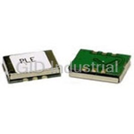
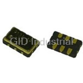
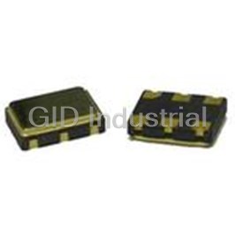
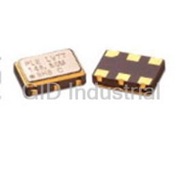
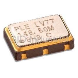
PLETRONICS LV1144BV-125.0M
Description
SMD Crystal Oscillator 125MHz 3.3V 6-Pin SMD
LV1144BV-125.0M
Part Number
LV1144BV-125.0M
Price
Request Quote
Manufacturer
PLETRONICS
Lead Time
Request Quote
Category
Frequency Controls » SMD Crystal Oscillator
Specifications
Manufacturer
Pletronics
Manufacturers Part #
LV1144BV-125.0M
Industry Aliases
LV1144BV-125.0M
Sub-Category
SMD Crystal Oscillators
Factory Pack Quantity
1
Datasheet

Extracted Text
LV11B Series 3.3 V LVDS Clock Oscillators January 2014 This device is supported for legacy designs only, LV11B is not recommended for new designs. • Pletronics’ LV11B Series is a quartz crystal • 80 to 700 MHz controlled precision square wave generator with • 9.9mm x 13.97mm ‘B’ package an LVDS output. • Enable/Disable Function on pad 2 • Solder pad compatible with many 9x14 Plastic J- • Does NOT permit “wired-OR” of outputs lead packages. • Low Jitter • FR4 base may or may not have a mechanical metal cover. • Tape and Reel or cut tape packaging is available. Pletronics Inc. certifies this device is in accordance with the RoHS 6/6 (2002/95/EC) and WEEE (2002/96/EC) directives. Pletronics Inc. guarantees the device does not contain the following: Cadmium, Hexavalent Chromium, Lead, Mercury, PBB’s, PBDE’s Weight of the Device: 2.18 grams or .82 grams or 1.51 grams Moisture Sensitivity Level: 1 As defined in J-STD-020C Second Level Interconnect code: e4 Absolute Maximum Ratings: Parameter Unit V Supply Voltage -0.5V to +7.0V CC Vi Input Voltage -0.5V to V + 0.5V CC Vo Output Voltage -0.5V to V + 0.5V CC Thermal Characteristics o The maximum die or junction temperature is 155 C o The thermal resistance junction to board is 60 to 100 C/Watt depending on the solder pads, ground plane and construction of the PCB. Product information is current as of publication date. The product conforms Copyright © 2006, 2007, 2008 Pletronics Inc. to specifications per the terms of the Pletronics standard warranty. Production processsing does not necessarily include testing of all parameters. LV11B Series 3.3 V LVDS Clock Oscillators January 2008 Part Number: LV11 45 B E V -125.0M -XX Part Marking: Packaging code or blank PLE T250 = 250 per Tape and Reel LV11B T500 = 500 per Tape and Reel FFFF.F M T1K = 1000 per Tape and Reel CCCC YMDXX or Frequency in MHz LV11BX FFFF.F M Supply Voltage V CC PLE XX V = 3.3V _ + 10% CC YYWWXX CC Optional Enhanced OTR o Blank = Temp. range -10 to +70 C o E = Temp. range -40 to +85 C Series Model Frequency Stability 45 = _ + 50 ppm 44 = _ + 25 ppm 20 = _ + 20 ppm Series Model Legend: PLE = Pletronics FFFF.F M = Frequency in MHz YMD or YYWW = Date of Manufacture (Year - month - day or year and week) All other marking is internal factory codes Specifications such as frequency stability, supply voltage and operating temperature range, etc. are not identified from the marking. External packaging labels and packing list will correctly identify the ordered Pletronics part number. Codes for Date Code YMD Code 6 7 8 9 0 1 2 2006 2007 2008 2009 2010 2011 2012 Year Code A B C D E F G H J K L M JAN FEB MAR APR MAY JUN JUL AUG SEP OCT NOV DEC Month Code 1 2 3 4 5 6 7 8 9 A B C Day 1 2 3 4 5 6 7 8 9 10 11 12 Code D E F G H J K L M N P R Day 13 14 15 16 17 18 19 20 21 22 23 24 Code T U V W X Y Z 25 26 27 28 29 30 31 Day www.pletronics.com 425-776-1880 2 LV11B Series 3.3 V LVDS Clock Oscillators January 2008 Electrical Specification for 3.30V + _10% over the specified temperature range Item Min Max Unit Condition Frequency Range 1 700 MHz Frequency Accuracy “45" -50 +50 ppm For all supply voltages, load changes, aging for 1 year, shock, vibration and temperatures -25 +25 “44" -20 +20 “20" Output Waveform LVDS Output High Level -- 1.60 Volts Output Low Level 0.90 -- Volts Differential Output (V ) 250 450 mVolts See load circuit R1 = 50 ohms OD Output Offset Voltage (V ) 1.125 1.375 Volts > 80 MHz OS Differential Output Error (dV ) -- 50 mVolts OS Output Symmetry 45 55 % Referenced to 50% of amplitude or crossing point Output T and T 300 700 pS > 80 MHz RISE FALL Vth is 20% and 80% of waveform 400 900 pS < 80 MHz Jitter - 0.2 pS RMS Measured from 12KHz to 20MHz from Fnominal - 2.8 Measured from 10Hz to 1MHz from Fnominal Vcc Supply Current - 90 mA > 80 MHz Includes current of properly terminated device Enable/Disable Internal Pull-up 50 - Kohm To Vcc (equivalent resistance) V disable - 0.8 Volts Referenced to Ground V enable 2.0 - Volts Enable - 100 nS Time for output to reach a logic state Disable time - 100 nS Time for output to reach a high Z state Start up time - 5 mS > 80 MHz Measured from the time Vcc = 3.0V o Operating Temperature Range -10 +70 C Standard Temperature Range o -40 +85 C Extended Temperature Range “E” Option o Storage Temperature Range -55 +125 C Specifications with Pad 2 E/D open circuit www.pletronics.com 425-776-1880 3 LV11B Series 3.3 V LVDS Clock Oscillators January 2008 Typical Phase-Noise Response 0 -20 -40 -60 -80 -100 -120 -140 -160 10 1,000 100,000 10,000,000 Frequency (Hz) Load Circuit Test Waveform Symmetry Vhigh Out 80% 50% 20% Vlow Out* Trise Tfall www.pletronics.com 425-776-1880 4 dBc/Hz LV11B Series 3.3 V LVDS Clock Oscillators January 2008 Reliability: Environmental Compliance Parameter Condition Mechanical Shock MIL-STD-883 Method 2002, Condition B Vibration MIL-STD-883 Method 2007, Condition A Solderability MIL-STD-883 Method 2003 Thermal Shock MIL-STD-883 Method 1011, Condition A ESD Rating Model Minimum Voltage Conditions Human Body Model 1500 MIL-STD-883 Method 3115 Charged Device Model 1000 JESD 22-C101 Package Labeling Label is 1" x 2.6" (25.4mm x 66.7mm) Label is 1" x 2.6" (25.4mm x 66.7mm) Font is Courier New Font is Arial Bar code is 39-Full ASCII Layout and application information Recommend connecting Pad 1 and Pad 2 together to permit the design to accept Enable/Disable on both input pads For Optimum Jitter Performance, Pletronics recommends: • a ground plane under the device • no large transient signals (both current and voltage) should be routed under the device • do not layout near a large magnetic field such as a high frequency switching power supply • do not place near piezoelectric buzzers or mechanical fans. www.pletronics.com 425-776-1880 5 LV11B Series 3.3 V LVDS Clock Oscillators January 2008 Mechanical: Inches mm A 0.390 + _0.010 9.90 + _0.25 B 0.550 + _0.010 13.97 + _0.25 C 0.125 max 3.17 max 1 D 0.026 typ. 0.66 1 E 0.050 1.27 1 F 0.028 R 0.72 R 1 G 0.180 4.57 FR4 PCB Base: Cover: Solder masked 1 Centered on the base H 0.100 2.54 All via holes tented on bottom 304 Stainless Steel Copper Clad ½ oz. Typical 1 0.010 inch (0.25µm) I 0.050 1.27 Gold plated 0.02 µinch (0.5 µm) Electroless Nickel Plated Label: 1 1 µinch (25 µm) typical J 0.015 0.38 White Kapton with Black Letters –or-- 1 Pin 3 Ground plane is typical K 0.380 9.65 Blue Epoxy heat cure ink covering top with laser marked lettering Not to scale • The package is not hermetically sealed. • This device may not have a cover. • The sides are intentionally left open to permit cleaning material to freely flow in the package, thus minimizing the accumulation of contaminants during cleaning processes. • The internal part of the package must be thoroughly dry before operating. Pad Function Note 1 No connect There is no internal connection to this pad Output When this pad is not connected the oscillator shall operate. 2 Enable/Disable When this pad is <0.30 volts, the output will be inhibited (high impedance state.) Recommend connecting this pad to V if the oscillator is to be always on. CC 3 Ground (GND) 4 Output The outputs must be terminated, 100 ohms between the outputs is the ideal termination. When disabled, the outputs are not in a high impedance state - can 5 Output* not be wire - or connected 6 Supply Voltage Recommend connecting appropriate power supply bypass capacitors as close as (V ) possible. CC www.pletronics.com 425-776-1880 6 LV11B Series 3.3 V LVDS Clock Oscillators January 2008 Reflow Cycle (typical for lead free processing) 245°C Maximum 10 Seconds Maximum 250 215°C±10°C 200 175°C±10°C 150 100 120 to 160 Seconds Approximately 50 Seconds Allowed rate of temperature change Maximum 4°C per second The part may be reflowed 2 times without degradation. Tape and Reel: available for quantities of 250 to 1000 per reel, cut tape for < 250 Constant Dimensions Table 1 T1 Tape D1 S1 D0 E1 P0 P2 T Max Max Size Min Min 8mm 1.0 2.0 + _0.05 1.5 12mm 1.5 1.75 4.0 0.6 0.6 0.1 +0.1 + _0.1 + _0.1 16mm 1.5 2.0 -0.0 + _0.1 24mm 1.5 Variable Dimensions Table 2 Tape B1 E2 Min F P1 T2 W Ao, Bo Size Max Max Max & Ko 24 mm 12.1 14.25 7.5 + _0.1 16.0 + _0.1 8.0 16.3 Note 1 Note 1: Embossed cavity to conform to EIA-481-B Dimensions in mm Not to scale REEL DIMENSIONS A inches 7.0 10.0 13.0 mm 177.8 254.0 330.2 B inches 2.50 4.00 3.75 mm 63.5 101.6 95.3 Tape Width C mm 13.0 +0.5 / -0.2 D mm --- --- 24.4 24.0 +2.0 -0.0 Reel dimensions may vary from the above www.pletronics.com 425-776-1880 7 Temperature (°C) LV11B Series 3.3 V LVDS Clock Oscillators January 2008 IMPORTANT NOTICE Pletronics Incorporated (PLE) reserves the right to make corrections, improvements, modifications and other changes to this product at anytime. PLE reserves the right to discontinue any product or service without notice. Customers are responsible for obtaining the latest relevant information before placing orders and should verify that such information is current and complete. All products are sold subject to PLE’s terms and conditions of sale supplied at the time of order acknowledgment. PLE warrants performance of this product to the specifications applicable at the time of sale in accordance with PLE’s limited warranty. Testing and other quality control techniques are used to the extent PLE deems necessary to support this warranty. Except where mandated by specific contractual documents, testing of all parameters of each product is not necessarily performed. PLE assumes no liability for application assistance or customer product design. Customers are responsible for their products and applications using PLE components. To minimize the risks associated with the customer products and applications, customers should provide adequate design and operating safeguards. PLE products are not designed, intended, authorized or warranted to be suitable for use in life support applications, devices or systems or other critical applications that may involve potential risks of death, personal injury or severe property or environmental damage. Inclusion of PLE products in such applications is understood to be fully at the risk of the customer. Use of PLE products in such applications requires the written approval of an appropriate PLE officer. Questions concerning potential risk applications should be directed to PLE. PLE does not warrant or represent that any license, either express or implied, is granted under any PLE patent right, copyright, artwork or other intellectual property right relating to any combination, machine or process which PLE product or services are used. Information published by PLE regarding third-party products or services does not constitute a license from PLE to use such products or services or a warranty or endorsement thereof. Use of such information may require a license from a third party under the patents or other intellectual property of the third party, or a license from PLE under the patents or other intellectual property of PLE. Reproduction of information in PLE data sheets or web site is permissible only if the reproduction is without alteration and is accompanied by associated warranties, conditions, limitations and notices. Reproduction of this information with alteration is an unfair and deceptive business practice. PLE is not responsible or liable for such altered documents. Resale of PLE products or services with statements different from or beyond the parameters stated by PLE for that product or service voids all express and implied warranties for the associated PLE product or service and is an unfair or deceptive business practice. PLE is not responsible for any such statements. Contacting Pletronics Inc. Pletronics Inc. Tel: 425-776-1880 th 19013 36 Ave. West Fax: 425-776-2760 Lynnwood, WA 98036-5761 USA E-mail: ple-sales@pletronics.com URL: www.pletronics.com Copyright © 2005, 2006, Pletronics Inc. www.pletronics.com 425-776-1880 8
Frequently asked questions
How does Electronics Finder differ from its competitors?

Is there a warranty for the LV1144BV-125.0M?
Which carrier will Electronics Finder use to ship my parts?
Can I buy parts from Electronics Finder if I am outside the USA?
Which payment methods does Electronics Finder accept?
Why buy from GID?

Quality
We are industry veterans who take pride in our work

Protection
Avoid the dangers of risky trading in the gray market

Access
Our network of suppliers is ready and at your disposal

Savings
Maintain legacy systems to prevent costly downtime

Speed
Time is of the essence, and we are respectful of yours
Related Products
Oscillator XO 125MHz ±25ppm LVDS 55% 2.5V 6-Pin CLLCC SMD LV5544DEW-125.0M
Oscillator XO 100MHz ±20ppm LVDS 55% 3.3V 6-Pin CLLCC SMD LV7720DV-100.0M
SMD Crystal Oscillator 100MHz 2.5V 6-Pin CLCC LV7720DW-100.0M
Oscillator XO 125MHz ±20ppm LVDS 55% 2.5V 6-Pin CLLCC SMD LV7720DW-125.0M
Oscillator XO 125MHz ±25ppm LVDS 55% 3.3V 6-Pin CLLCC SMD LV7744DEV-125.0M
Oscillator XO 156.25MHz ±25ppm LVDS 55% 3.3V 6-Pin CLLCC SMD LV7744DEV-156.25M
Request a Quote

The quote request has been received
Close

Facing challenges or have inquiries? Feel free to contact us!
Call Us +1-469-283-2440
What they say about us
FANTASTIC RESOURCE
One of our top priorities is maintaining our business with precision, and we are constantly looking for affiliates that can help us achieve our goal. With the aid of GID Industrial, our obsolete product management has never been more efficient. They have been a great resource to our company, and have quickly become a go-to supplier on our list!
Bucher Emhart Glass
EXCELLENT SERVICE
With our strict fundamentals and high expectations, we were surprised when we came across GID Industrial and their competitive pricing. When we approached them with our issue, they were incredibly confident in being able to provide us with a seamless solution at the best price for us. GID Industrial quickly understood our needs and provided us with excellent service, as well as fully tested product to ensure what we received would be the right fit for our company.
Fuji
HARD TO FIND A BETTER PROVIDER
Our company provides services to aid in the manufacture of technological products, such as semiconductors and flat panel displays, and often searching for distributors of obsolete product we require can waste time and money. Finding GID Industrial proved to be a great asset to our company, with cost effective solutions and superior knowledge on all of their materials, it’d be hard to find a better provider of obsolete or hard to find products.
Applied Materials
CONSISTENTLY DELIVERS QUALITY SOLUTIONS
Over the years, the equipment used in our company becomes discontinued, but they’re still of great use to us and our customers. Once these products are no longer available through the manufacturer, finding a reliable, quick supplier is a necessity, and luckily for us, GID Industrial has provided the most trustworthy, quality solutions to our obsolete component needs.
Nidec Vamco
TERRIFIC RESOURCE
This company has been a terrific help to us (I work for Trican Well Service) in sourcing the Micron Ram Memory we needed for our Siemens computers. Great service! And great pricing! I know when the product is shipping and when it will arrive, all the way through the ordering process.
Trican Well Service
GO TO SOURCE
When I can't find an obsolete part, I first call GID and they'll come up with my parts every time. Great customer service and follow up as well. Scott emails me from time to time to touch base and see if we're having trouble finding something.....which is often with our 25 yr old equipment.
ConAgra Foods