

 Manufacturers
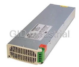
GE CRITICAL POWER CP3000AC54TEZ
Description
CP3000AC54TEZ, 3000W, -54V, UNIVERSAL AC INPUT, TOTAL EFFICIENCY
Part Number
CP3000AC54TEZ
Price
Request Quote
Manufacturer
GE CRITICAL POWER
Lead Time
Request Quote
Category
Circuit Protection » AC-DC Power Supply
Specifications
Manufacturer
GE Critical Power
Manufacturers Part #
CP3000AC54TEZ
Industry Aliases
150033916
Brand
GE Critical Power
Series
CP3000AC54TE
Factory Pack Quantity
1
Cooling Method
Air-Cooled
Dimensions
13.83 x 4.00 x 1.63"
Efficiency
96%
Isolation
3000 VAC
Mechanical Style
Open / Enclosed Frame
Mounting
Rack Mount
Operating Temperature
- 10 to + 75°C
Output Amps 1
55.5 A
Power
3000 W
Subcategory
AC-DC Power Supply
Datasheet

Extracted Text
Data sheet GE CP3000/3500AC54TE Global Platform High Efficiency Rectifier Input: 100-120/200-277 Vac; Default Output: ±54 Vdc @ 3000W/3500W; 5 Vdc @ 10W Features RoHS Compliant Efficiency meets 80plus Titanium requirements 3 Compact 1RU form factor with 40 W/in density Constant power from 52 – 58VDC 3000 or 3500W from nominal 200-277VAC 1500W from nominal 100 – 120V AC Output voltage programmable from 42V – 58VDC ON/OFF control of the main output Comprehensive input, output and overtemp. protection 2 PMBus compliant dual I C serial bus and RS485 Precision measurement reporting such as input power Applications consumption, input/output voltage & current Remote firmware upgrade capable 48VDC distributed power architectures Routers/ VoIP/Soft and other Telecom Switches Power factor correction (meets EN/IEC 61000-3-2 and EN 60555-2 requirements) LAN/WAN/MAN applications Redundant, parallel operation with active load sharing File servers, Enterprise Networks, Indoor wireless Redundant +5V @ 2A Aux power SAN/NAS/iSCSI applications Internally controlled Variable-speed fan Hot insertion/removal (hot plug) Four front panel LED indicators † UL* Recognized, CAN/ CSA C22.2 to IEC60950-1, § CE mark meets 2006/95/EC directive CB report available Description The CP3000/3500AC54TEP Rectifiers provide significantly higher power density in the same form factor and efficiency improvements in the Compact Power Line of Rectifiers. The only difference between these rectifiers is output power limit. High- density front-to-back airflow is designed for minimal space utilization and is highly expandable for future growth. Wide-input enables the rectifier to be deployed internationally into a wide range of commercially available voltage sources. Configured with 2 both dual-redundant I C and RS485 based communications busses, so that it could be positioned into a broad range of applications. Feature set flexibility makes this rectifier an excellent choice for applications requiring modular AC to - 48V DC intermediate voltages, such as in distributed power. * UL is a registered trademark of Underwriters Laboratories, Inc. † CSA is a registered trademark of Canadian Standards Association. ‡ VDE is a trademark of Verband Deutscher Elektrotechniker e.V. § This product is intended for integration into end-user equipment. All CE marking procedures of end-user equipment should be followed. (The CE mark is placed on selected products.) ** ISO is a registered trademark of the International Organization of Standards + The PMBus name and logo are registered trademarks of the System Management Interface Forum (SMIF) July 22, 2016 ©2016 General Electric Company. All rights reserved. Data sheet GE CP3000/3500AC54TE Global Platform High Efficiency Rectifier Input: 100-120/200-277 Vac; Default Output: ±54 Vdc @ 3500W; 5 Vdc @ 10W Absolute Maximum Ratings Stresses in excess of the absolute maximum ratings can cause permanent damage to the device. These are absolute stress ratings only, functional operation of the device is not implied at these or any other conditions in excess of those given in the operations sections of the data sheet. Exposure to absolute maximum ratings for extended periods can adversely affect the device reliability. Parameter Symbol Min Max Unit Input Voltage: Continuous VIN 0 300 VAC 1 Operating Ambient Temperature TA -10 75 °C Storage Temperature Tstg -40 85 °C I/O Isolation voltage to Frame (100% factory Hi-Pot tested) 1500 VAC Electrical Specifications Unless otherwise indicated, specifications apply over all operating input voltage, Vo=54V , resistive load, and temperature DC conditions. INPUT Parameter Symbol Min Typ Max Unit Startup Voltage Low-line Operation 80 85 90 High-line Operation 185 Operating Voltage Range Low-line Configuration 90 100 – 120 140 V V IN AC High-line Configuration 185 200 - 277 300 Voltage Swell (no damage) 305 Turn OFF Voltage 75 80 85 Hysteresis 5 Frequency FIN 47 66 Hz Source Impedance (NEC allows 2.5% of source voltage drop inside a 0.2 Ω building) Operating Current; at 110V 15.5 AC IIN AAC at 240VAC 16 Inrush Transient (220VRMS , 25°C, excluding X-Capacitor charging) IIN 25 40 APK 9 Idle Power (at 240VAC, 25C) 54V OFF PIN W 54V ON @ Io=0 18 Leakage Current (300V , 60Hz) I 2.5 3.5 mA AC IN Power Factor (50 – 100% load) PF 0.97 0.995 2 Efficiency , 240VAC @ 25C 10% of FL 90 94 20% of FL % 50% of FL 96 FL 91 Holdup time (output allowed to decay down to 40V ) 10 DC T ms For loads below 1500W 15 Ride through (at 240V 25C) T 1/2 1 cycle AC, 3 Power Good Warning (main output allowed to decay to 40VDC) PG 3 5 ms Isolation (per EN60950) (consult factory for testing to this requirement) Input-Chassis/Signals V 1500 V AC Input - Output 3000 V AC 1 See the derating guidelines under the Environmental Specifications section 2 Fan disabled, 5V output at 0 load. 3 Internal protection circuits may override the PG signal and may trigger an immediate shutdown. PG should not indicate normal (HI) until the main output is within regulation. PG should be asserted if the main output is about to shut down for any detectible reason. July 22, 2016 ©2016 General Electric Company. All rights reserved. Page 2 Data sheet GE CP3000/3500AC54TE Global Platform High Efficiency Rectifier Input: 100-120/200-277 Vac; Default Output: ±54 Vdc @ 3500W; 5 Vdc @ 10W Electrical Specifications (continued) 54VDC MAIN OUTPUT Parameter Symbol Min Typ Max Unit Output Power @ low line input 100 – 120V 1500 AC W WDC @ high line input 200 – 277VAC 3000/3500 Factory set default set point 54 VDC Overall regulation (load, temperature, aging) 0 - 45C LOAD > 2.5A -1 +1 % > 45C VOUT -2 +2 4 Output Voltage Set Range - analog margining 44 58 VDC 2 - Set either by I C or RS485 42 58 Output Current - @ 1500W (100 – 120Vac), 54V/52V 1 27.8/28.9 @ 3000W (200 – 277VAC), 54V/52V I 1 55.5/57.8 A Out DC @ 3500W (200 – 277VAC), 54V/52V 1 64.8/67.3 Current Share ( > 50% FL) -5 5 %FL 5 Proportional Current Share between different rectifiers ( > 50% FL) <7 %FL Output Ripple ( 20MHz bandwidth, load > 1A) RMS (5Hz to 20MHz) 100 mV rms V OUT 6 Peak-to-Peak (5Hz to 20MHz) 250 mVp-p 7 Psophometric Noise 9 mVrms External Bulk Load Capacitance C 0 5,000 F OUT Turn-On (monotonic turn-ON from 30 – 100% of Vnom above 5C) Delay 5 s T 100 ms Rise Time – PMBus mode 8 Rise Time - RS-485 mode 5 s Output Overshoot VOUT 2 % Load Step Response ( I > 2.5A ) O,START 9 I IOUT 50 %FL V, VAC 285AC VOUT 2.0 VDC V 3.2 V V, VAC ≥ 285AC OUT DC T 2 ms Response Time Overload - Power limit @ high line down to 52VDC P 3000/3500 W OUT DC Power limit @ low line down to 52VDC P 1500 W OUT DC 10 High line current limit if Vout > 39VDC [3000W/3500W] IOUT 59/68 ADC Low line current limit IOUT 30 ADC Output shutdown (commences as voltage decays below this level) VOUT 36 VDC System power up Upon insertion the rectifier will delay an overload shutdown for 20 seconds allowing for the insertion and startup of multiple rectifiers within a system. Overvoltage - 200ms delayed shutdown < 60 VOUT VDC Immediate shutdown > 65 Latched shutdown Three restart attempts are implemented within a 1 minute window prior to a latched shutdown. 5 Over-temperature warning (prior to commencement of shutdown) Shutdown (below the max device rating being protected) T 20 C Restart attempt Hysteresis (below shutdown level) 10 Isolation Output-Chassis (Standard, non-POE compliant) 500 VDC V Output-Chassis/Signals (POE compliant per IEEE802.3) 2250 VDC 4 When VO > 57VDC or when VIN > 270VAC and VO < 48VDC power derating starts at 50C 5 With existing CP platform of rectifiers 6 500mVp-p max above 280VAC , 300mVp-p max for POE product 7 Complies with ANSI TI.523-2001 section 4.9.2 emissions max limit of 20mV flat unweighted wideband noise limits 8 Below -5°C, the rise time is approximately 5 minutes to protect the bulk capacitors. Rise time can be changed to 100ms, contact factory for details. 9 di/dt (output current slew rate) 1A/µs. 10 Above 280V the current limit reduces to 50A when V ≤ 45V and to 25A when V ≤ 45V and T > 55C. AC OUT DC OUT DC AMB July 22, 2016 ©2016 General Electric Company. All rights reserved. Page 3 Data sheet GE CP3000/3500AC54TE Global Platform High Efficiency Rectifier Input: 100-120/200-277 Vac; Default Output: ±54 Vdc @ 3500W; 5 Vdc @ 10W 5VDC Auxiliary output Parameter Symbol Min Typ Max Unit Output Voltage Setpoint V 5 V OUT DC Overall Regulation -3 +3 % Output Current 0.005 2 A Ripple and Noise (20mHz bandwidth) 50 100 mVp-p Over-voltage Clamp 7 VDC Over-current Limit 110 175 %FL The 5VDC should be ON before availability of the 54VDC main output and should turn OFF only if insufficient input voltage exists to provide reliable 5VDC power. The PG# signal should have indicated a warning that power would get turned OFF and the 54VDC main output should be OFF way before interruption of the 5V output. DC General Specifications Parameter Min Typ Max Units Notes Full load, 25C ; MTBF per SR232 Reliability protection for Reliability 450,000 Hours electronic equipment, issue 2, method I, case III, Service Life 10 Years Full load, excluding fans Unpacked Weight 2.18/4.8 Kgs/Lbs Packed Weight 2.45/5.4 Kgs/Lbs Heat Dissipation 190 Watts or 648 BTUs @ 80% load, 250 Watts or 853 BTUs @ 100% load Signal Specifications Unless otherwise indicated, specifications apply over all operating input voltage, resistive load, and temperature conditions. Signals are referenced to Logic_GRD unless noted otherwise. Fault, PG#, OTW, Alert, SCL, SDA need to be pulled HI by external pull-up resistors. Max sink current: 5mA Parameter Symbol Min Typ Max Unit ON/OFF 54V output OFF VOUT 0.7VDD 5 VDC 54V output ON (should be connected to Logic_GRD) VOUT 0 0.5 VDC Margining (through adjusting Vprog) 44 58 V DC Voltage control range Vcontrol 0 3.3 VDC Programmed output voltage range VOUT 44 58 VDC Voltage adjustment resolution (8-bit A/D) V 3.3 mV control DC Output configured to 54VDC Vcontrol 3.0 3. 3 VDC Output configured to 44VDC Vcontrol 0 0.1 VDC 11 V ≤ 10VDC, settling time to new value Tcontrol 150 200 ms Interlock [short pin shorted to VOUT( - ) on system side] Module Present [short pin shorted to Logic_GRD internally] Over Temperature Warning (OTW#) Logic HI (temperature normal) V 0.7VDD 12 VDC Sink current [note: open collector output FET] I 5 mA Logic LO (temperature is too high) V 0 0.4 VDC Power Good (PG) Logic HI (normal) [ open collector output FET} V 0.7V 12 V DD DC Logic LO (temperature is too high) V 0 0.4 VDC Protocol select Logic HI - Analog/PMBus™ mode V 2.7 3.5 V IH DC Logic – intermediate – RS485 mode V 1.0 2.65 V II DC Logic LO – DSP reprogram mode V 0 0.4 V IL DC Fault# Logic HI (No fault is present) V 0.7VDD 12 VDC Logic LO (Fault is present) V 0 0.4 V DC Alert# (Alert#_0, Alert#_1) Logic HI (No Alert - normal) V 0.7VDD 12 VDC Logic LO (Alert# is set) V 0 0.4 VDC SCL, SDA (SCL_0/1, SDA_0/1) Logic HI V 0.7V 12 V DD DC Logic LO (Alert# is set) V 0 0.4 V DC 11 Reducing the output voltage may take longer at light load due to capacitive discharge July 22, 2016 ©2016 General Electric Company. All rights reserved. Page 4 Data sheet GE CP3000/3500AC54TE Global Platform High Efficiency Rectifier Input: 100-120/200-277 Vac; Default Output: ±54 Vdc @ 3500W; 5 Vdc @ 10W Digital Interface Specifications Parameter Conditions Symbol Min Typ Max Unit 12 PMBus Signal Interface Characteristics Input Logic High Voltage (CLK, DATA) V 1.5 3.6 VDC Input Logic Low Voltage (CLK, DATA) V 0 0.8 V DC Input high sourced current (CLK, DATA) I 0 10 μA Output Low sink Voltage (CLK, DATA, ALERT#) I=3.5mA V 0.4 V OUT DC Output Low sink current (CLK, DATA, ALERT#) I 3.5 mA Output High open drain leakage current (CLK,DATA, V=3.6V I 0 10 μA OUT ALERT#) PMBus Operating frequency range Slave Mode FPMB 10 400 kHz Measurement System Characteristics Clock stretching Tstretch 25 ms I measurement range I 0 80 A OUT rng DC > 12.8A -1 +1 % of FL I measurement accuracy 25°C I OUT out(acc) < 12.8A 5 5 % 13 I measurement accuracy 0 - 40°C > 12.8A I -2 +2 % of FL OUT out(acc) V measurement range V 0 70 V OUT out(rng) DC 14 VOUT measurement accuracy Vout(acc) -1 +1 % Temp measurement range Temp(rng) 0 150 C 15 Temp measurement accuracy Temp(acc) -4 +4 C V measurement range V 0 320 V IN in(rng) AC V > 120V -1.25 +1.25 IN AC V measurement accuracy @ 25°C V % IN in(acc) VIN < 120VAC -2 2 I measurement range I 0 30 I IN in(rng) AC I measurement accuracy - IN Iin(acc) -4 +4 % of FL standard measurement @ 25°C > 1A -2.5 2.5 % IIN measurement accuracy - I in(acc) improved measurement @ 25°C ≤ 1A -400 400 mA P measurement range P 0 4000 W IN in(rng) in > 350W +5 % PIN measurement accuracy – -5 P in(acc) standard measurement @ 25°C < 350W 35 50 W > 500W -1.5 1 +1.5 % PIN measurement accuracy – 100 – 500W Pin(acc) -2.0 1.5 +2.0 % improved measurement @ 25°C < 100W -20 15 20 W Fan Speed measurement range 0 30k RPM Fan Speed measurement accuracy -10 10 % Fan speed control range 0 100 % 12 Clock, Data, and Alert# need to be pulled up to VDD externally. 13 Below 20% of FL; 10 – 20% of FL: ±0.64A; 5 – 10% of FL: ±0.45A; 2.5 – 5% of FL: ±0.32A. 14 Above 2.5A of load current 15 Within 30 of the default warning and fault levels. July 22, 2016 ©2016 General Electric Company. All rights reserved. Page 5 Data sheet GE CP3000/3500AC54TE Global Platform High Efficiency Rectifier Input: 100-120/200-277 Vac; Default Output: ±54 Vdc @ 3500W; 5 Vdc @ 10W Environmental Specifications Parameter Min Typ Max Units Notes 16 17 Ambient Temperature -40 55 °C Air inlet from sea level to 5,000 meters. Exhaust Air Temperature 15 °C Maximum allowed internal temperature rise Storage Temperature -40 85 °C Operating Altitude 5000/16400 m / ft Non-operating Altitude 8200/30000 m / ft Power Derating with Temperature 2.0 %/°C 55°C to 75C Acoustic noise 55 dbA Full load Over Temperature Protection 125/11 Shutdown / restart [internally measured °C 0 points] Humidity Operating 5 95 % Relative humidity, non-condensing Storage 5 95 % IPC-9592B, Class II Shock and Vibration acceleration 2.4 Grms EMC Parameter Measurement Standard Level Test Conducted emissions EN55022, FCC Docket 20780 part 15, subpart J A +6dB 0.15 – 30MHz Meets Telcordia GR1089-CORE by a 3dB margin 18 AC input Radiated emissions EN55022 A +6dB 30 – 10000MHz Line harmonics EN61000-3-2 Table 1 0 – 2 KHz 5% THD (230V, FL, 25C) 19 Parameter Measurement Standard Criteria Test Line sags and EN61000-4-11 B -30%, 10ms interruptions B -60%, 100ms B -100%, 5sec Output will stay above 40VDC @ 75% load 25% line sag for 2 seconds A AC Input Sag must be higher than 80Vrms. 1 cycle interruption Immunity Lightning surge EN61000-4-5, Level 4, 1.2/50µs – error free A 4kV, common mode A 2kV, differential mode ANSI C62.41 - level A3 B 6kV, common & differential Fast transients EN61000-4-4, Level 3 B 5/50ns, 2kV (common mode) Conducted RF fields EN61000-4-6, Level 3 A 130dBµV, 0.15-80MHz, 80% AM Radiated RF fields EN61000-4-3, Level 3 A 10V/m, 80-1000MHz, 80% AM Enclosure immunity ENV 50140 A ESD EN61000-4-2, Level 4 B 8kV contact, 15kV air 16 Designed to start and work at an ambient as low as -40°C, but may not meet operational limits until above -5°C 17 At 277V input line operation the maximum ambient is reduced to 50C. See operational limitations in other sections of this document 18 Emissions requirements can be verified using either the J2007001 or J85480 GE shelf. Standalone the additional margin is not required. 19 Criteria A: The product must maintain performance within specification limits. Criteria B: Temporary degradation which is self recoverable. Criteria C: Temporary degradation which requires operator intervention. July 22, 2016 ©2016 General Electric Company. All rights reserved. Page 6 Data sheet GE CP3000/3500AC54TE Global Platform High Efficiency Rectifier Input: 100-120/200-277 Vac; Default Output: ±54 Vdc @ 3500W; 5 Vdc @ 10W Characteristic Curves o The following figures provide typical characteristics for the CP3500AC54TE rectifier and 25 C. 230VIN @ 25C 110VIN @ 25C OUTPUT CURRENT, I (A) OUTPUT CURRENT O Figure 1. Rectifier Efficiency versus Output Current. Figure 2. Inrush current VIN = 230VAC, 0C phase angle OUTPUT CURRENT Figure 3. 54V output: Power limit, Current limit and Figure 4. 54V output: Power limit, Current limit and DC DC shutdown profile at VIN = 90VAC. shutdown profile at VIN = 185VAC. TIME, t (10ms /div) TIME, t (10ms/div) Figure 5. 54V output ripple and noise, full load, Figure 6. 5V output ripple and noise, all full load, DC DC V = 185V , 20MHz bandwidth V = 185V , 20MHz bandwidth IN AC IN AC July 22, 2016 ©2016 General Electric Company. All rights reserved. Page 7 OUTPUT VOLTAGE OUTPUT VOLTAGE EFFICIENCY, (%) VO (V) (200mV/div) OUTPUT VOLTAGE V – Red I - Yellow IN IN V (V) (20mV/div) OUTPUT VOLTAGE O VIN – (200V/div) IIN – (10A/div) Data sheet GE CP3000/3500AC54TE Global Platform High Efficiency Rectifier Input: 100-120/200-277 Vac; Default Output: ±54 Vdc @ 3500W; 5 Vdc @ 10W Characteristic Curves (continued) o The following figures provide typical characteristics for the CP3500AC54TE rectifier and 25 C. TIME, t (2ms/div) Time, t (50ms/div) Figure 7. Transient response 54V load step 10 – 60%, Figure 8. Transient response 54V load step 10 – 60%, DC DC Slew rate: 1A/µs, V = 230V Slew rate: 1A/µs, V = 230V . IN AC IN AC TIME, t (200ms/div) TIME, t (2s/div) Figure 9. 54V soft start delay when ON/OFF is asserted, Figure 10. 54V soft start, full load, V = 230V - DC DC IN AC 2 V =230V - I C mode. RS485 mode with 4700µf external capacitance. IN AC TIME, t (10ms/div) TIME, t (5ms/div) Figure 11. Ride through missing ½ cycle, full load, Figure 12. PG# alarmed 10ms prior to Vo < 40V, V = 230V . V = 230V , Output at Full load IN AC IN AC July 22, 2016 ©2016 General Electric Company. All rights reserved. Page 8 54V OUT – Red ON/OFF - Green IOUT - Green VOUT - Red INPUT VOLTAGE OUUTPUT VOLTAGE VO (10V/div) on/off (1V/div) IO (V) (50A/div) VO(500mV/div) VIN (V) (100V/div) VO(V) (10V/div) PG - Red OUUTPUT - Green I - Green V - Red OUT OUT OUTPUT VOLTAGE V (V) (5V/div) V (V) (10V/div) I (V) (50A/div) V (500mV/div) PG O O O VO (V) (10V/div) Data sheet GE CP3000/3500AC54TE Global Platform High Efficiency Rectifier Input: 100-120/200-277 Vac; Default Output: ±54 Vdc @ 3500W; 5 Vdc @ 10W Characteristic Curves (continued) o The following figures provide typical characteristics for the CP3500AC54TE rectifier and 25 C. Power Good# TIME, t (20ms/div) TIME, t (1s/div) Figure 13. 40ms AC dropout @ full load, V = 230V . Figure 14. Turn-ON at full load V = 230V . IN AC IN AC Power Good# TIME, t (500ms/div) TIME, t (200ms/div) Figure 15. Turn-OFF at full load, V =230V Figure 16. 54V turn-OFF delay when ON/OFF is di- IN AC DC 2 asserted, V =230V - I C mode. IN AC INPUT VOLTAGE Figure 17. Output power derating below V of 185V IN AC July 22, 2016 ©2016 General Electric Company. All rights reserved. Page 9 54VOUT - Yellow 5VOUT - Blue 54VOUT - Yellow 5VOUT - Green 54VO(10V/div) 5VO (1V/div) 54VO(10V/div) 5VO (1V/div) OUTPUT POWER 54VOUT - Yellow 5VOUT - Blue 54V OUT – Red ON/OFF - Green 54VO(10V/div) 5VO (1V/div) VO (10V/div) on/off (1V/div) Data sheet GE CP3000/3500AC54TE Global Platform High Efficiency Rectifier Input: 100-120/200-277 Vac; Default Output: ±54 Vdc @ 3500W; 5 Vdc @ 10W Timing diagrams Response to input fluctuations T1 – ride through time – 0.5 to 1 cycles [ 10 – 20ms] VOUT remains within regulation – load dependent T2 – hold up time - 15ms – V stays above 40V OUT DC 2 T3 – delay time – 10s – from when the AC returns within regulation to when the output starts rising in I C mode 2 T4 – rise time - 120ms – the time it takes for V to rise from 10% to 90% of regulation in I C mode OUT T5 – power good warning – 3ms – the time between assertion of the PG signal and the output decaying below 40VDC. T6 – hold up time of the 5VAUX output @ full load – 1s – from the time AC input failed T7 – rise time of the 5VAUX output - 3.65ms – 5VAUX is available at least 450ms before the main output is within regulation Blinking of the input/AC LED – V < 80V (the low transitioned signal represents blinking of the input LED. IN AC July 22, 2016 ©2016 General Electric Company. All rights reserved. Page 10 Data sheet GE CP3000/3500AC54TE Global Platform High Efficiency Rectifier Input: 100-120/200-277 Vac; Default Output: ±54 Vdc @ 3500W; 5 Vdc @ 10W bits, up to sixteen (16) rectifiers can be independently Control and Status addressed on a single I²C bus. These four bits are configured The Rectifier provides three means for monitor/control: by two signal pins, Unit_ID and Rack_ID. The least analog, PMBus™, or the GE Galaxy-based RS485 protocol. significant bit x (LSB) of the address byte is set to either Details of analog control and the PMBus™ based protocol write [0] or read [1]. A write command instructs the rectifier. are provided in this data sheet. GE will provide separate A read command accesses information from the rectifier. application notes on the Galaxy RS485 based protocol for users to interface to the rectifier. Contact your local GE Address Bit Assignments representative for details. Device Address (Most to Least Significant) 7 6 5 4 3 2 1 0 Control hierarchy: Some features, such as output voltage, µP 40 – 4F 1 0 0 A3 A2 A1 A0 R/W can be controlled both through hardware and firmware. For Broadcast 00 0 0 0 0 0 0 0 0 example, the output voltage is controlled both by a signal MSB LSB pin (Vprog) and firmware (Vout_command; 0x21). Unit_ID: Up to 10 different units are selectable. Using output voltage as an example, the Vprog signal pin Inside power supply voltage level sets the output voltage if its value is A voltage divider between 3.3V < 3VDC. (see the Vprog section). When the programming 3.3Vdc and Logic_GRD configures Unit_ID. signal Vprog is either a no connect or > 3VDC, the output Internally a 10kΩ resistor is pulled voltage is set at the default value of 54V . DC up to 3.3VDC. A pull down resistor 10k Rs needs to be connected between The signal pin controls the feature it is configuring until a Unit_ID pin Unit_ID and Logic_GRD. firmware command is executed. However, once the firmware command has been executed, the signal pin is ignored. In the above example, the rectifier will no longer Rs ‘listen’ to the Vprog pin if the Vout_command has been Logic_GRD executed. In summary, signals such as Vprog are utilized for setting Unit_ID Voltage level R (± 0.1%) S the initial default value and for varying the value until firmware based control takes over. Once firmware control is Invalid 3.30 executed, hardware based control is relinquished so the 1 3.00 100k processor can clearly decide who has control. 2 2.67 45.3k 3 2.34 24.9k Analog controls: Details of analog controls are provided in 4 2.01 15.4k this data sheet under Feature Specifications. 5 1.68 10.5k Signal Reference: Unless otherwise noted, all signals are 6 1.35 7.15k referenced to Logic_GRD. See the Signal Definitions Table at the end of this document for further description of all the 7 1.02 4.99k signals. 8 0.69 2.49k Logic_GRD is isolated from the main output of the rectifier 9 0.36 1.27k for PMBus communications. Communications and the 5V 10 0 0 standby output are not connected to main power return (Vout(-)) and can be tied to the system digital ground point selected by the user. (Note that RS485 communications is Rack_ID: Up to 8 different combinations are selectable. referenced to Vout(-), main power return of the rectifier). Inside power supply Logic_GRD is capacitively coupled to Frame_GRD inside the A voltage divider between 5Vdc rectifier. The maximum voltage differential between 5VDC and Logic_GRD configures Rack_ID. The Logic_GRD and Frame_GRD should be less than 100VDC. 10k 10k-20kΩ divider sets the initial voltage level to 3.3VDC. Rack_ID Control Signals A switch between each R S value changes the Rack_ID Protocol: This signal pin defines the communications mode Rs 20k level according to the table setting of the rectifier. Two different states can be below. Logic_GRD 2 configured. State #1 is the I C application in which case the protocol pin should be left a no-connect. State #2 is the RS485 mode application in which case a resistor value between 1kΩ and 5kΩ should be present between this pin and Vout ( - ). 2 Device address in I C mode: Address bits A3, A2, A1, A0 set the specific address of the µP in the rectifier. With these four July 22, 2016 ©2016 General Electric Company. All rights reserved. Page 11 Data sheet GE CP3000/3500AC54TE Global Platform High Efficiency Rectifier Input: 100-120/200-277 Vac; Default Output: ±54 Vdc @ 3500W; 5 Vdc @ 10W Device address in RS485 mode: The address in RS485 mode is divided into three components; Bay_ID, Slot_ID and Rack_ID Voltage level R (± 0.1%) S Shelf_ID 1 3.3 open 2 Bay_ID: The Unit_ID definition in I C mode becomes the bay 2 2.8 35.2k id in RS485 mode. 3 2.3 15k 4 1.8 8k Slot_ID: Up to 10 different rectifiers could be positioned 5 1.4 4.99k across a 19” shelf if the rectifiers are located vertically within 6 1 2.87k the shelf. The resistor below needs to be placed between Slot_ID and Vout ( - ). Internal pull-up to 3.3V is 10kΩ. 7 0.5 1.27k 8 0 0 Slot Resistor Voltage Slot Resistor Voltage invalid none 3.3V 6 7.15k 1.35V 1 100k 3V 7 4.99k 1.02V Configuration of the A3 – A0 bits: The rectifier will 2 45.3k 2.67V 8 2.49k 0.69V determine the configured address based on the Unit_ID and 3 24.9k 2.34V 9 1.27k 0.36V Rack_ID voltage levels as follows (the order is A3 – A0): 4 15.4k 2.01V 10 0 0 5 10.5k 1.68V Unit_ID Shelf_ID: When placed horizontally up to 10 shelves can be 1 2 3 4 5 stacked on top of each other in a fully configured rack. The shelf will generate the precision voltage level tabulated 1 0000 0001 0010 0011 below referenced to Vout ( - ). 0100 0101 0110 0111 2 1000 1001 1010 1011 3 Shelf VMIN VNOM VMAX 1100 1101 1110 1111 4 1 2.3 2.5 2.7 Rack_ID 2 4.7 5.0 5.3 5 3 7.4 7.5 7.6 6 0000 0001 0010 0011 0100 4 9.5 10.0 10.5 0101 0110 0111 1000 1001 7 5 11.8 12.5 13.2 8 1010 1011 1100 1101 1110 6 14.2 15.0 15.8 7 16.6 17.5 18.4 Unit x Rack: 4 x 4 and 5 x 3 8 19 20.0 21 9 21.3 22.5 23.6 10 23.8 25.0 26.3 Unit_ID 6 7 8 9 10 Global Broadcast: This is a powerful command because it 0000 0001 1 instruct all rectifiers to respond simultaneously. A read 0010 0011 2 instruction should never be accessed globally. The rectifier should issue an ‘invalid command’ state if a ‘read’ is 0100 0101 3 attempted globally. 0110 0111 0000 0001 0010 4 Rack_ID 5 1000 1001 0011 0100 0101 For example, changing the ‘system’ output voltage requires the global broadcast so that all paralleled rectifiers change 1010 1011 0110 0111 1000 6 their output simultaneously. This command can also turn 1001 1010 1011 7 1100 1101 OFF the ‘main’ output or turn ON the ‘main’ output of all 1110 1111 1100 1101 1110 8 rectifiers simultaneously. Unfortunately, this command does have a side effect. Only a single rectifier needs to pull down the ninth acknowledge bit. To be certain that each Unit x Rack: 2 x 8 and 3 x 5 rectifier responded to the global instruction, a READ instruction should be executed to each rectifier to verify that Address detection: The Slot_ID pin must be shorted to the command properly executed. The GLOBAL BROADCAST Vout(-) in order to deliver output power. This connection command should only be executed for write instructions to provides a second interlock feature. (In RS485 mode the slave devices. slot_ID resistance to Vout(-) is sufficient to sense the interlock feature) Voltage programming (V ): Hardware voltage prog programming controls the output voltage until a software command to change the output voltage is executed. Software voltage programming permanently overrides the hardware margin setting and the rectifier no longer listens July 22, 2016 ©2016 General Electric Company. All rights reserved. Page 12 Data sheet GE CP3000/3500AC54TE Global Platform High Efficiency Rectifier Input: 100-120/200-277 Vac; Default Output: ±54 Vdc @ 3500W; 5 Vdc @ 10W to any hardware margin settings until power to the Status Signals controller is interrupted, for example if input power or bias Module Present: This signal is tied to Logic_GRD inside the power is recycled. rectifier. It’s intent is to provide a signal to the system that a rectifier is physically present in the slot. When bias power is recycled to the controller the controller restarts into its default configuration, programmed to set Power Good Warning (PG#): This signal is HI when the the output as instructed by the V pin. Again, subsequent prog main output is being delivered and goes LO if the main software commanded settings permanently override the output is about to decay below regulation. Note that should margin setting. As an example, adding a resistor between a catastrophic failure occur, the signal may not be fast Vprog and Logic_GRD is an effective way of changing the enough to provide a meaningful warning. PG# also pulses factory set point of the rectifier to whatever voltage level is at a 1ms duty cycle if the unit is in overload. desired by the user during initial start-up. Fault#: A TTL compatible status signal representing The Vprog pin level should be set by a divider from 3.3Vdc to whether a Fault occurred. This signal needs to be pulled HI Logic_GRD external to the rectifier as shown in the graph. externally through a resistor. This signal goes LO for any Programming can be accomplished either by a resistor failure that requires rectifier replacement. These faults may divider or by a voltage source injecting a precision voltage be due to: level into the Vprog pin. Above 3Vdc the rectifier sets the Fan failure output to its default state. Over-temperature shutdown An analog voltage on this signal can vary the output voltage Over-voltage shutdown from 44Vdc to 58Vdc. Internal Rectifier Fault -58 Over temp warning (OTW#): A TTL compatible status signal representing whether an over temperature exists. This signal -54 needs to be pulled HI externally through a resistor. -46 If an over temperature should occur, this signal would pull -44 Vprog LO for approximately 10 seconds prior to shutting down the rectifier. In its default configuration, the unit would restart if internal temperatures recover within normal operational levels. At that time the signal reverts back to its open collector (HI) state. 0 0.1 Power_CAP: This signal is HI when the main output is 3000w Vprog (Vdc) and goes LO when the main output is 1400w. Factory default setting driven by Vprog Serial Bus Communications Load share (Ishare): This is a single wire analog signal that is generated and acted upon automatically by rectifiers The I²C interface facilitates the monitoring and control of connected in parallel. Ishare pins should be connected to various operating parameters within the unit and transmits each other for rectifiers, if active current share among the these on demand over an industry standard I²C Serial bus. rectifiers is desired. No resistors or capacitors should get connected to this pin. All signals are referenced to ‘Logic_GRD’. ON/OFF: Controls the main 54VDC output when either Pull-up resistors: The clock, data, and Alert# lines do not analog control or PMBus protocols are selected, as have any internal pull-up resistors inside the rectifier. The configured by the Protocol pin. This pin must be pulled low customer is responsible for ensuring that the transmission to turn ON the rectifier. The rectifier will turn OFF if either the 2 impedance of the communications lines complies with I C ON/OFF or the Interlock pin is released. This signal is and SMBus standards. referenced to Logic_GRD. Note that in RS485 mode this pin is ignored. Serial Clock (SCL): The clock pulses on this line are generated by the host that initiates communications across Interlock: This is a shorter pin utilized for hot-plug applications to ensure that the rectifier turns OFF before the the I²C Serial bus. This signal needs to be pulled HI externally power pins are disengaged. It also ensures that the rectifier through a resistor as necessary to ensure that rise and fall turns ON only after the power pins have been engaged. time timing and the maximum sink current is in compliance Must be connected to V_OUT ( - ) for the rectifier to be ON. to the I²C /SMBus specifications. 8V_INT: Single wire connection between rectifiers, Provides Serial Data (SDA): This line is a bi-directional data line. This bias to the DSP of an unpowered rectifier. signal needs to be pulled HI externally through a resistor as July 22, 2016 ©2016 General Electric Company. All rights reserved. Page 13 Output Setpoint (Vdc) Inside module Data sheet GE CP3000/3500AC54TE Global Platform High Efficiency Rectifier Input: 100-120/200-277 Vac; Default Output: ±54 Vdc @ 3500W; 5 Vdc @ 10W necessary to ensure that rise and fall time timing and the The host controller needs to recognize this clock stretching, maximum sink current is in compliance to the I²C /SMBus and refrain from issuing the next clock signal, until the clock specifications. line is released, or it needs to delay the next clock pulse beyond the clock stretch interval of the rectifier. Note that clock stretching can only be performed after completion of SMBUSAlert#: This hardware signal pin is normally HI. th transmission of the 9 ACK bit, the exception being the When asserted (logic LO) it signifies to the system controller START command. that the state of the power supply has changed or that communication errors occurred. The SMBusAlert# line exciting the rectifier combines the Alert# functions of rectifier control and dual_bus_control. Digital Feature Descriptions Clock Stretch PMBus™ compliance: The rectifier is fully compliant to the Figure 15. Example waveforms showing clock stretching. Power Management Bus (PMBus™) rev1.2 requirements. This Specification can be obtained from www.pmbus.org. I²C Bus Lock-Up detection: The device will abort any transaction and drop off the bus if it detects the bus being ‘Manufacturer Specific’ commands are used to support held low for more than 35ms. additional instructions that are not in the PMBus™ specification. Communications speed: Both 100kHz and 400kHz clock All communication over the PMBus interface must support rates are supported. The rectifiers default to the 100kHz the Packet Error Checking (PEC) scheme. The PMBus master clock rate. must generate the correct PEC byte for all transactions, and check the PEC byte returned by the rectifier. Packet Error Checking (PEC): The rectifier will not respond to commands without the trailing PEC. The integrity of Non-volatile memory is used to store configuration settings. communications is compromised if packet error correction Not all settings programmed into the device are is not employed. There are many functional features, automatically saved into this non-volatile memory. Only including turning OFF the main output, that require those specifically identified as capable of being stored can validation to ensure that the desired command is executed. be saved. (see the Table of Commands for which command parameters can be saved to non-volatile storage). PEC is a CRC-8 error-checking byte, based on the polynomial 8 2 C(x) = x + x + x + 1, in compliance with PMBus™ requirements. The calculation is based in all message bytes, Non-supported commands: Non supported commands are including the originating write address and command bytes flagged by setting the appropriate STATUS bit and issuing an preceding read instructions. The PEC is appended to the Alert# to the ‘host’ controller. message by the device that supplied the last byte. If a non-supported read is requested the rectifier will return 0x00h for data. Alert#: The rectifier can issue Alert# driven from either its 2 internal micro controller (µC) or from the I C bus master Data out-of-range: The rectifier validates data settings and selector stage. That is, the Alert# signal of the internal µC sets the data out-of-range bit and Alert# if the data is not funnels through the master selector stage that buffers the within acceptable range. Alert# signal and splits the signal to the two Alert# signal pins exiting the rectifier. In addition, the master selector Master/Slave: The ‘host controller’ is always the MASTER. stage signals its own Alert# request to either of the two Rectifiers are always SLAVES. SLAVES cannot initiate Alert# signals when required. communications or toggle the Clock. SLAVES also must respond expeditiously at the command of the MASTER as The µC driven Alert# signal informs the ‘master/host’ required by the clock pulses generated by the MASTER. controller that either a STATE or ALARM change has occurred. Normally this signal is HI. The signal will change to its LO level if the rectifier has changed states and the signal Clock stretching: The ‘slave’ µController inside the rectifier will be latched LO until the rectifier receives a ‘clear_faults’ may initiate clock stretching if it is busy and it desires to instruction. delay the initiation of any further communications. During the clock stretch the ‘slave’ may keep the clock LO until it is The signal will be triggered for any state change, including ready to receive further instructions from the host controller. the following conditions; The maximum clock stretch interval is 25ms. VIN under or over voltage Vout under or over voltage July 22, 2016 ©2016 General Electric Company. All rights reserved. Page 14 Data sheet GE CP3000/3500AC54TE Global Platform High Efficiency Rectifier Input: 100-120/200-277 Vac; Default Output: ±54 Vdc @ 3500W; 5 Vdc @ 10W IOUT over current sequentially control the rectifier. For example, a short or an 2 open connection in one of the I C lines does not affect Over Temperature warning or fault 2 communications capability on the other I C line. Failure of a Fan Failure ‘master’ controller does not affect the rectifiers and the Communication error second ‘master’ can take over control at any time. PEC error Invalid command Conceptually a Digital Signal Processor (DSP) referenced to Internal faults Vout(-) of the rectifier provides secondary control. A Both Alert#_0 and -1 are asserted during power up to Bidirectional Isolator provides the required isolation notify the master that a new rectifier has been added between power GRD, Vout(-) and signal GRD (Logic_GRD). A to the bus. secondary micro controller provides instructions to and receives operational data from the DSP. The secondary The rectifier will clear the Alert# signal (release the signal to micro controller also controls the communications over two its HI state) upon the following events: 2 independent I C lines to two independent system controllers. Receiving a CLEAR_FAULTS command 2 Bias power to the processor is recycled I C_0 Bidirectional DSP µC The rectifier will re-assert the Alert line if the internal state of Isolator the rectifier has changed, even if that information cannot be 2 IC1 reported by the status registers until a clear_faults is issued by the host. If the Alert asserts, the host should respond by The secondary micro controller is designed to default to 2 issuing a clear_faults to retire the alert line (this action also I C_0 when powered up. If only a single system controller is 2 utilized, it should be connected to I C_0. In this case the provides the ability to change the status registers). This 2 I C_1 line is totally transparent as if it does not exist. action triggers another Alert assertion because the status registers changed states to report the latest state of the If two independent system controllers are utilized, then one rectifier. The host is now able to read the latest reported 2 of them should be connected to I C_0 and the other to status register information and issue a clear_faults to retire 2 I C_1. the Alert signal. 2 At power up the master connected to I C_0 has control of 2 Re-initialization: The I C code is programmed to re-initialize the bus. See the section on Dual Master Control for further if no activity is detected on the bus for 5 seconds. Re- description of this feature. 2 initialization is designed to guarantee that the I C µController does not hang up the bus. Although this rate is longer than the timing requirements specified in the SMBus specification, it had to be extended in order to ensure that a re-initialization would not occur under normal transmission rates. During the few µseconds required to accomplish re- 2 initialization the I C µController may not recognize a command sent to it. (i.e. a start condition). Read back delay: The rectifier issues the Alert# notification 2 Conceptual representation of the dual I C bus system. as soon as the first state change occurred. During an event a number of different states can be transitioned to before the final event occurs. If a read back is implemented rapidly TM by the host a successive Alert# could be triggered by the PMBus Commands transitioning state of the rectifier. In order to avoid successive Alert# s and read back and also to avoid reading Standard instruction: Up to two bytes of data may follow a transitioning state, it is prudent to wait more than 2 an instruction depending on the required data content. seconds after the receipt of an Alert# before executing a Analog data is always transmitted as LSB followed by MSB. read back. This delay will ensure that only the final state of PEC is mandatory and includes the address and data fields. the rectifier is captured. 1 8 1 8 1 S Slave address Wr A Command Code A Successive read backs: Successive read backs to the rectifier should not be attempted at intervals faster than 8 1 8 1 8 1 1 every one second. This time interval is sufficient for the Low data byte A High data byte A PEC A P internal processors to update their data base so that Master to Slave Slave to Master successive reads provide fresh data. SMBUS annotations; S – Start , Wr – Write, Sr – re-Start, Rd – Read, Dual Master Control: A – Acknowledge, NA – not-acknowledged, P – Stop 2 Two independent I C lines provide true communications bus redundancy and allow two independent controllers to July 22, 2016 ©2016 General Electric Company. All rights reserved. Page 15 Data sheet GE CP3000/3500AC54TE Global Platform High Efficiency Rectifier Input: 100-120/200-277 Vac; Default Output: ±54 Vdc @ 3500W; 5 Vdc @ 10W Standard READ: Up to two bytes of data may follow a READ Standard features request depending on the required data content. Analog data is always transmitted as LSB followed by MSB. PEC is Supported features that are not readable: The commands mandatory and includes the address and data fields. below are supported at the described setting but they cannot be read back through the command set. 1 7 1 1 8 1 Command Comments S Slave address Wr A Command Code A ON_OFF_CONFIG (0x02) Both the CNTL pin, and the OPERATION command, enabling or 1 7 1 1 8 1 disabling the output, are supported. Sr Slave Address Rd A LSB A Other options are not supported. Capability (0x19) 400KHz, ALERT# 8 1 8 1 1 PMBus revision (0x98) 1.2 MSB A PEC NA P Block communications: When writing or reading more than Status and Alarm registers: The registers are updated with two bytes of data at a time BLOCK instructions for WRITE the latest operational state of the rectifier. For example, and READ commands are used instead of the Standard whether the output is ON or OFF is continuously updated Instructions above to write or read any number of bytes with the latest state of the rectifier. However, alarm greater than two. information is maintained until a clear_faults command is received from the host. For example, the shutdown or Block write format: OC_fault bits stay in their alarmed state until the host clears 1 7 1 1 8 1 the registers. S Slave address Wr A Command Code A 8 1 8 1 8 1 A clear_faults clears all registers. If a fault still persists after Byte count = N A Data 1 A Data 2 A the clear_faults is commanded, the register bit annunciating the fault is reset again. 8 1 8 1 8 1 1 ………. A Data N A PEC A P TM PMBus Command set: Block read format: Non-volatile 1 7 1 1 8 1 Memory S Slave address Wr A Command Code A 20 storage Hex Data Command Code Field & default 1 7 1 1 Operation 0x01 1 Yes/80 Sr Slave Address Rd A Clear_Faults 0x03 - 8 1 8 1 8 1 Write _Protect 0x10 1 Yes/00 Byte count = N A Data 1 A Data 2 A Restore_default_all 0x12 - Restore_user_all 0x16 - 8 1 8 1 8 1 1 Store_user_code 0x17 1 yes ………. A Data N A PEC NA P Restore_user_code 0x18 1 Vout_mode 0x20 1 Linear Data Format: The definition is identical to Part II of Vout_command 0x21 2 yes the PMBus Specification. All standard PMBus values, with Vin_ON 0x35 2 No/85 the exception of output voltage related functions, are Vin_OFF 0x36 2 No/80 represented by the linear format described below. Output Fan_config_1_2 0x3A 1 Yes /99 voltage functions are represented by a 16 bit mantissa. Fan_command_1 0x3B 2 Output voltage has a E=9 constant exponent. The Linear Data Format is a two byte value with an 11-bit, Vout_OV_fault_limit 0x40 2 Yes / 60 two’s complement mantissa and a 5-bit, two’s complement Vout_OV_fault_response 0x41 1 No / 80 exponent or scaling factor, its format is shown below. Vout_OV_warn_limit 0x42 2 Yes / 59 Data Byte High Data Byte Low Vout_UV_warn_limit 0x43 2 Yes / 42 Bit 7 6 5 4 3 2 1 0 7 6 5 4 3 2 1 0 Exponent (E) Mantissa (M) Vout_UV_fault_limit 0x44 2 Yes /41 Vout_UV_fault_response 0x45 1 No / C0 The relationship between the Mantissa, Exponent, and Iout_OC_fault_limit 0x46 2 Yes / 68 Actual Value (V) is given by the following equation: 21 Iout_OC_fault_response 0x47 1 Yes / F8 E VM2 Iout_OC_LV_fault_limit 0x48 2 Yes/36 Where: V is the value, M is the 11-bit, two’s complement mantissa, E is the 5-bit, two’s complement exponent 20 Yes – indicates that the data can be changed by the user 21 Only latched (0xC0) or hiccup (0xF8) are supported July 22, 2016 ©2016 General Electric Company. All rights reserved. Page 16 Data sheet GE CP3000/3500AC54TE Global Platform High Efficiency Rectifier Input: 100-120/200-277 Vac; Default Output: ±54 Vdc @ 3500W; 5 Vdc @ 10W Non-Volatile Non-Volatile Memory Memory Storage Storage Hex Data Hex Data Command Code Field & Default Command Code Field & Default Iout_OC_warn_limit 0x4A 2 Yes / 67.3 Test_Function 0xDF 1 OT_fault_limit 0x4F 2 Yes/TBD 22 OT_fault_response 0x50 1 Yes / C0 Upgrade commands OT_warn_limit 0x51 2 Yes/105 Password 0xE0 4 Vin_OV_fault_limit 0x55 2 No/ 300 Target_list 0xE1 4 Vin_OV_fault_response 0x56 1 No/ C0 Compatibility_code 0xE2 32 Vin_OV_warn_limit 0x57 2 Yes / 295 Software_version 0xE3 7 23 Vin_UV_warn_limit 0x58 2 Yes / 87.5 Memory_capability 0xE4 7 24 Vin_UV_fault_limit 0x59 2 No / 80 Application_status 0xE5 1 Vin_UV_fault_response 0x5A 1 No/ C0 Boot_loader 0xE6 1 Data_transfer 0xE7 ≤32 Status_byte 0x78 1 Product comcode 0xE8 11 Status_word (+ byte) 0x79 1 Status_Vout 0x7A 1 Upload_black_box 0xF0 ≤32 Status_Iout 0x7B 1 Status_Input 0x7C 1 Command set adjustment range Status_temperature 0x7D 1 Status_CML 0x7E 1 If a command is received for a value setting that is outside Status_fans_1_2 0x81 1 the range defined below, the module should not change the present setting. The module could NACK the command and Read_Vin 0x88 2 set the invalid/unsupported data bit of the status_cml (0x7E) Read_Iin 0x89 2 register. Read_Vout 0x8B 2 Default Adjustment range Read_Iout 0x8C 2 Hex Command Code HL (LL) Low High Read_temp_PFC 0x8D 2 Vout_command 0x21 54 41 59 Read_temp_dc_pri 0x8E 2 Fan_command_1 0x3B - 0 100 Read_temp_dc_sec 0x8F 2 Vout_OV_fault_limit 0x40 60 41 60 Read_fan_speed_1 0x90 2 Vout_OV_warn_limit 0x42 59 42 59 Read_fan_speed_2 0x91 2 Vout_UV_warn_limit 0x43 42 38 58 Read_Pin 0x97 2 Vout_UV_fault_limit 0x44 41 36 58 Mfr_ID 0x99 6 Iout_OC_fault_limit 0x46 68 (30) 0 68 Mfr_model 0x9A 16 Iout_OC_LV_fault_limit 0x48 41 36 58 Mfr_revision 0x9B 8 Iout_OC_warn_limit 0x4A 67.3(29.8) 0 67.3 Mfr_serial 0x9E 16 OT_fault_limit 0x4F 110 0 150 OT_warn_limit 0x51 105 0 150 Status_summary 0xD0 11 Vin_OV_fault_limit 0x55 300 90 300 Status_unit 0xD1 2 Vin_OV_warn_limit 0x57 295 90 295 Status_alarm 0xD2 3 Vin_UV_warn_limit 0x58 87.5 80 295 Read_fan_speed 0XD3 6 Vin_UV_fault_limit 0x59 80 70 295 Read_input 0xD4 5 Read_firmware_rev 0xD5 6 Read_run_timer 0xD6 3 Command Descriptions Status_bus 0xD7 1 Operation (0x01) : Turns the 54V output ON or OFF. The Take_over_bus_control 0xD8 default state is ON at power up. Only the following data EEPROM Record 0xD9 128 yes bytes are supported: Read_temp_exhaust 0xDA 2 FUNCTION DATA BYTE Read_ temp_inlet 0xDB 2 Unit ON 0x80 Reserved for factory use 0XDC Unit OFF 0x00 Reserved for factory use 0XDD Reserved for factory use 0XDE To RESET the rectifier using this command, command the rectifier OFF, wait at least 2 seconds, and then command the rectifier back ON. All alarms and shutdowns are cleared 22 during a restart. Only latched (0x80) or restart (0xC0) are supported 23 Recovery set at 90V 24 Recovery set at 86V July 22, 2016 ©2016 General Electric Company. All rights reserved. Page 17 Data sheet GE CP3000/3500AC54TE Global Platform High Efficiency Rectifier Input: 100-120/200-277 Vac; Default Output: ±54 Vdc @ 3500W; 5 Vdc @ 10W Clear_faults (0x03): Clears all STATUS and FAULT registers The default set point can be overridden by the Vprog signal 2 2 and resets the Alert# line of the I C side in control. The I C pin which is designed to override the firmware based default side not in control cannot clear registers in the rectifier. This setting during turn ON. command is always executable. In parallel operation, changing the output voltage should be If a fault still persists after the issuance of the clear_faults performed simultaneously to all rectifiers using the Global command, the specific registers indicating the fault first Address (Broadcast) feature. If only a single rectifier is clears but then get set again to indicate that the unit is still instructed to change its output, it may attempt to source all in the fault state. the required power which can cause either a power limit or shutdown condition. Software programming of output voltage permanently WRITE_PROTECT register (0x10): Used to control writing to overrides the set point voltage configured by the Vprog the PMBus device. The intent of this command is to provide signal pin. The program no longer looks at the ‘Vprog pin’ protection against accidental changes. All supported and will not respond to any hardware voltage settings. If commands may have their parameters read, regardless of power is removed from the µController it will reset itself into the write_protect settings. The contents of this register its default configuration looking at the Vprog signal for cannot be stored into non-volatile memory using the output voltage control. In many applications, the Vprog pin Store_user_code command. The default setting of this is used for setting initial conditions, if different that the register is enable_all_writes, write_protect 0x00h. The factory setting. Software programming then takes over once write_protect command must always be accepted. 2 I C communications are established. To properly hot-plug a rectifier into a live backplane, the FUNCTION DATA BYTE system generated voltage should get re-configured into Enable all writes 00 either the factory adjusted firmware level or the voltage Disable all writes except write_protect 80 level reconfigured by the Vprog pin. Otherwise, the voltage Disable all writes except write_protect and 40 state of the plugged in rectifier could be significantly OPERATION different than the powered system. Programmed voltage range: 42V – 58 V . DC DC Restore_default_all (0x12): Restores all operating register values and responses to the factory default parameters set in the rectifier. The factory default cannot be changed. A voltage programming example: The task: set the output voltage to 50.45VDC Restore_user_all (0x16): Restores all operating register values and responses to the user default parameters set in This rectifier supports the linear mode of conversion the rectifier. The user default can be changed. specified in the PMBus™ specification. The supported output voltage exponent is documented in the Vout_mode (0x20) -9 Store_user_code (0x17): Changes the user default setting of command. The exponent for output voltage setting is 2 a single register. In this fashion some protection is offered to (see the PMBus™ specification for reading this command). 9 ensure that only those registers that are desired to be Calculate the required voltage setting to be sent; 50.45 x 2 changed are in fact changed. = 25830. Convert this decimal number into its hex equivalent: 64E6 and send it across the bus LSB first and Restore_user_code (0x18): Restores the user default setting then MSB; E664 with the trailing PEC. of a single register. Vin_ON (0x35): This is a ‘read only’ register that informs the Vout_mode (0x20): This is a ‘read only’ register. The upper controller at what input voltage level the rectifier turns ON. three bits specify the supported data format, in this case The default value is tabulated in the data section. The value Linear mode. The lower five bits specify the exponent of the is contingent on whether the rectifier operates in the data in two’s complement binary format for output voltage low_line or high_line mode. related commands, such as Vout_command. These commands have a 16 bit mantissa. The exponent is fixed by the rectifier and is returned by this command Vin_OFF (0x36): This is a ‘read only’ register that informs the controller at what input voltage level the rectifier turns OFF. The default value is tabulated in the data section. The value is contingent on whether the rectifier operates in the Mode Bits [7:5] Bits [4:0] (Parameter) low_line or high_line mode. Linear 000b xxxxxb Vout_Command (0x21) : Used to dynamically change the Fan_config_1_2 (0x3A) : This command requires that the output voltage of the rectifier. This command can also be fan speed be commanded by duty cycle. Both fans must be used to change the factory programmed default set point of commanded simultaneously. The tachometer pulses per the rectifier by executing a store-user instruction that revolution is not used. Default is duty cycle control. changes the user default firmware set point. July 22, 2016 ©2016 General Electric Company. All rights reserved. Page 18 Data sheet GE CP3000/3500AC54TE Global Platform High Efficiency Rectifier Input: 100-120/200-277 Vac; Default Output: ±54 Vdc @ 3500W; 5 Vdc @ 10W Fan_command_1 (0x3B): This command instructs the Vout_UV_warn_limit (0x43): Sets the value at which a rectifier to increase the speed of both fans above what is warning will be issued that the output voltage is too low. internally required. The transmitted data byte represents Reduction below the warning value will set the Alert# signal. the hex equivalent of duty cycle in percentage, i.e. 100% = 0 x 64h. The command can increase or decrease fan speed. Vout_UV_fault_limit (0x44): Sets the value at which the An incorrect value will result in a ‘data error’. rectifier will shut down if the output gets below this level. Sending 00h tells the rectifier to revert back to its internal This register is masked if the UV is caused by interruption of control. the input voltage to the rectifier. Vout_OV_fault_limit (0x40): Sets the value at which the Vout_UV_fault_response (0x45): Sets the response if the main output voltage will shut down. output voltage falls below the UV_fault_limit. The default UV_fault_response is restart (0xC0). The only two allowable Vout_OV_fault_response (0x41): This is a ‘read only’ states are latched (0x80) and restart (0xC0). register. The only allowable state is a latched state after three retry attempts. Iout_OC_fault_limit (0x46): Sets the value at which the An overvoltage shutdown is followed by three attempted rectifier will shut down at High Line. This level can be restarts, each successive restart delayed 1 second. If within permanently changed and stored in non-volatile memory. a 1 minute window three attempted restarts failed, the unit The Low Line level is not adjustable. will latch OFF. If less than 3 shutdowns occur within the 1 minute window then the count for latch OFF resets and the 1 minute window starts all over again. This performance Iout_OC_fault_response (0x47): Sets the response if the cannot be changed. output overload exceeds the OC_Fault_limit value. The default OC_fault_response is hiccup (0xF8). The only two Restart after a latched state: Either of four restart allowable states are latched (0xC0) or hiccup. The response mechanisms is available; is the same for both low_line and high_line operations. The hardware pin ON/OFF may be cycled OFF and then ON. Iout_OC_warn_limit (0x4A): Sets the value at which the The unit may be commanded to restart via i2c through rectifier issues a warning that the output current is getting the Operation command by first turning OFF then too close to the shutdown level at high line. The Low Line turning ON . level is not adjustable. The third way to restart is to remove and reinsert the unit. The fourth way is to turn OFF and then turn ON ac OT_fault_limit (0x4F): Sets the value at which the rectifier power to the unit. responds to an OT event, sensed by the dc-sec sensor. The A successful restart clears all STATUS and ALARM registers. response is defined by the OT_fault_response register. A power system that is comprised of a number of rectifiers could have difficulty restarting after a shutdown event OT_fault_response (0x50): Sets the response if the output because of the non-synchronized behavior of the individual overtemperature exceeds the OT_Fault_limit value. The rectifiers. Implementing the latch-off mechanism permits a default OT_fault_response is hiccup (0xC0). The only two synchronized restart that guarantees the simultaneous allowable states are latched (0x80) or hiccup restart of the entire system. A synchronous restart can be implemented by; OT_warn_limit (0x51): Sets the value at which the rectifier Issuing a GLOBAL OFF and then a GLOBAL ON issues a warning when the dc-sec temperature sensor command to all rectifiers exceeds the warn limit. Toggling Off and then ON the ON/OFF signal, if this Vin_OV_fault_limit (0x55): Sets the value at which the signal is paralleled among the rectifiers. rectifier shuts down because the input voltage exceeds the Removing and reapplying input commercial power to allowable operational limit. the entire system. Vin_OV_fault_response (0x56): Sets the response if the The rectifiers should be OFF for at least 20 – 30 seconds in input voltage level exceeds the Vin_OV_fault_limit value. order to discharge all internal bias supplies and reset the The default Vin_OV_fault_response is restart (0xC0). The only soft start circuitry of the individual rectifiers. two allowable states are latched (0x80) and restart (0xC0). Vin_UV_warn_limit (0x58): This is another warning flag Vout_OV_warn_limit (0x42): Sets the value at which a indicating that the input voltage is decreasing dangerously warning will be issued that the output voltage is too high. close to the low input voltage shutdown level. Exceeding the warning value will set the Alert# signal. Vin_UV_fault_limit (0x59): Sets the value at which the rectifier shuts down because the input voltage falls below the allowable operational limit. July 22, 2016 ©2016 General Electric Company. All rights reserved. Page 19 Data sheet GE CP3000/3500AC54TE Global Platform High Efficiency Rectifier Input: 100-120/200-277 Vac; Default Output: ±54 Vdc @ 3500W; 5 Vdc @ 10W STATUS_INPUT (0X7C): Returns one byte of information of input voltage related faults. Vin_UV_fault_response (0x5A): Sets the response if the Bit Default input voltage level falls below the Vin_UV_fault_limit value. Flag Position Value The default Vin_UV_fault_response is restart (0xC0). The only 7 VIN_OV_Fault 0 two allowable states are latched (0x80) and restart (0xC0). 6 VIN_OV_Warning 0 5 VIN_UV_ Warning 0 STATUS_BYTE (0x78) : Returns one byte of information with 4 VIN_UV_Fault 0 a summary of the most critical device faults. 3 Unit OFF for low input voltage 0 Bit Default 2 X 0 Flag Position Value 1 - 0 X 0 7 Unit is busy 0 6 OUTPUT OFF 0 5 VOUT Overvoltage Fault 0 STATUS_TEMPERATURE (0x7D): Returns one byte of 4 IOUT Overcurrent Fault 0 information of temperature related faults. 3 VIN Undervoltage Fault 0 Bit Default Flag 2 Temperature Fault or Warning 0 Position Value 1 CML (Comm. Memory Fault) 0 7 OT Fault 0 0 None of the above 0 6 OT Warning 0 5 - 0 X 0 STATUS_WORD (0x79): Returns status_byte as the low byte and the following high_byte. STATUS_CML (0X7E): Returns one byte of information of Bit Default communication related faults. Flag Position Value Bit Default Flag 7 VOUT Fault or Warning 0 Position Value 6 IOUT Fault or Warning 0 7 Invalid/Unsupported Command 0 5 INPUT Fault or Warning 0 6 Invalid/Unsupported Data 0 4 MFR SPECIFIC 0 5 Packet Error Check Failed 0 3 POWER_GOOD# (is negated) 0 4 - 2 X 0 2 FAN Fault or Warning 0 1 Other Communication Fault 0 1 OTHER 0 0 X 0 0 UNKNOWN Fault or Warning 0 STATUS_fans_1_2 (0X81): Returns one byte of information STATUS_VOUT (0X7A): Returns one byte of information of of fan status. output voltage related faults. Bit Default Flag Bit Default Position Value Flag Position Value 7 Fan 1 Fault 0 7 VOUT OV Fault 0 6 Fan 2 Fault 0 6 VOUT_OV_WARNING 0 5 - 4 Not supported 0 5 VOUT_UV_WARNING 0 3 Fan 1 speed overwritten 0 4 VOUT UV Fault 0 2 Fan 2 speed overwritten 0 3 - 0 X 0 1 - 0 Not supported 0 STATUS_IOUT (0X7B): Returns one byte of information of Read back Descriptions output current related faults. Bit Default Flag Single parameter read back: Functions can be read back Position Value one at a time using the read_word_protocol with PEC. A 7 IOUT OC Fault 0 command is first sent out notifying the slave what function 6 IOUT OC LV Fault 0 is to be read back followed by the data transfer. 5 IOUT OC Warning 0 4 X 0 Analog data is always transmitted LSB followed by MSB. A NA following the PEC byte signifies that the transmission is 3 CURRENT SHARE Fault 0 complete and is being terminated by the ‘host’. 2 IN POWER LIMITING MODE 0 1 - 0 X 0 1 8 1 8 1 S Slave address Wr A Command Code A The OC Fault limit sets where current limit is set. The rectifier actually shuts down below the LV fault limit setting. 1 8 1 Sr Slave address Rd A July 22, 2016 ©2016 General Electric Company. All rights reserved. Page 20 Data sheet GE CP3000/3500AC54TE Global Platform High Efficiency Rectifier Input: 100-120/200-277 Vac; Default Output: ±54 Vdc @ 3500W; 5 Vdc @ 10W Mfr_Specific Status and alarm registers: The content and 8 1 8 1 8 1 1 partitioning of these registers is significantly different than LSB A MSB A PEC No-Ack P the standard register set in the PMBus™ specification. More information is provided by these registers and they are either accessed rapidly, at once, using the ‘multi parameter’ Read back error: If the µC does not have sufficient time to read back scheme of this document, or in batches of two retrieve the requested data, it has the option to return all STATUS and two ALARM registers. FF’s instead of incorrect data. Read_fan_speed 1 & 2 (0x90, 0x91): Reading the fan speed Status_summary (0xD0) : This ‘manufacturer specific’ is in Direct Mode returning the RPM value of the fan. command is the basic read back returning STATUS and ALARM register data, output voltage, output current, and internal temperature data in a single read. Internal Read_FRU_ID (0x99,0x9A,0x9B,0x9E): Returns FRU temperature should return the temperature that is closest to information. Must be executed one register at a time. a shutdown level. 1 8 1 8 1 1 8 1 8 1 S Slave address Wr A Command Code A S Slave address Wr A Command 0x9x A 1 8 1 8 1 Sr Slave address Rd A Byte count = 11 A 1 8 1 8 1 Sr Slave address Rd A Byte count = x A 8 1 8 1 8 1 8 1 Status-2 A Status-1 A Alarm-3 A Alarm-2 A 8 1 8 1 8 1 8 1 1 Byte_1 A Byte A Byte_x A PEC No-Ack P 8 1 8 1 8 1 Alarm-1 A Voltage LSB A Voltage MSB A Mfr_ID (0x99): Manufacturer in ASCII – 6 characters 8 1 8 1 maximum, Current-LSB A Current-MSB A General Electric – Critical Power represented as, GE-CP 8 1 8 1 Temperature-LSB A Temperature-MSB A Mfr_model (0x9A): Manufacturer model-number in ASCII – 8 1 1 16 characters, for this unit: CP3500AC54TExxxx PEC No-Ack P Mfr_revision (0x9B): Total 8 bytes, this is the product series Status_unit(0xD1): This command returns the STATUS-2 and taking the form X:YZ. Each byte is in ASCII format. Read STATUS-1 register values using the standard ‘read’ format. from left to right, scanned in from the series number bar Status-2 code. Unused characters are filled at the end with null Bit Default Flag Position Value Mfr_serial (0x9E): Product serial number includes the 7 PEC Error 0 manufacturing date, manufacturing location in up to 16 6 OC [hiccup=1,latch=0] 1 characters. For example: 5 Invalid_Instruction 0 13KZ51018193xxx, is decoded as; 4 Power_Capacity [HL = 1] x 3 OR’ing Test Failed 0 13 – year of manufacture, 2013 2 n/a 0 KZ – manufacturing location, in this case Matamoros 1 Data_out_of_range 0 51 – week of manufacture 0 Remote ON/OFF [HI = 1] x 018193xxx – serial #, mfr choice Oring fault: Triggered either by the host driven or’ing test or by the repetitive testing of this feature within the rectifier. A TM destructive fault would cause an internal shutdown. Success Manufacturer-Specific PMBus Commands of the host driven test depends on power capacity capability Many of the manufacturer-specific commands read back which needs to be determined by the external processor. more than two bytes. If more than two bytes of data are Thus a non-destructive or’ing fault does not trigger a TM returned, the standard SMBus Block read is utilized. In this shutdown. process, the Master issues a Write command followed by the data transfer from the rectifier. The first byte of the Block Status-1 Read data field sends back in hex format the number of Bit Default data bytes, exclusive of the PEC number, that follows. Flag Position Value Analog data is always transmitted LSB followed by MSB. A 7 OT [Hiccup=1, latch=0] 1 No-ack following the PEC byte signifies that the transmission is complete and is being terminated by the ‘host’. 6 OR’ing_Test_OK 0 5 Internal_Fault 0 July 22, 2016 ©2016 General Electric Company. All rights reserved. Page 21 Data sheet GE CP3000/3500AC54TE Global Platform High Efficiency Rectifier Input: 100-120/200-277 Vac; Default Output: ±54 Vdc @ 3500W; 5 Vdc @ 10W 4 Shutdown 0 8 1 8 1 8 1 8 1 3 Service LED ON 0 Adj%-LSB A Adj%-MSB A Fan1-LSB A Fan1-MSB A 2 External_Fault 0 1 LEDs_Test_ON 0 8 1 8 1 8 1 1 0 Output ON (ON = 1) x Fan2-LSB A Fan2-MSB A PEC No-Ack P Status_alarm (0xD2): This command returns the ALARM-3 - Read input string (0xD4): Reads back the input voltage and ALARM-1 register values. input power consumed by the rectifier. Alarm-3 1 7 1 1 8 Bit Default S Slave address Wr A Command Code 0xDC Flag Position Value 7 Interlock open 0 1 1 7 1 1 6 Fuse fail 0 A Sr Slave Address Rd A 5 PFC-DC communications fault 0 2 8 1 8 1 8 1 4 DC-I C communications fault 0 Byte Count = 4 A Voltage - LSB A Voltage - MSB A 3 AC monitor communications fault 0 2 x 0 8 1 8 1 8 1 1 1 x 0 Power - LSB A Power - MSB A PEC No-Ack P 0 Or’ing fault 0 Alarm-2 Read_firmware_rev [0 x D5]: Reads back the firmware Bit Default revision of all three µC in the rectifier. Flag Position Value 7 FAN_Fault 0 1 7 1 1 8 1 6 No_Primary 0 S Slave address Wr A Command Code 0xDD A 5 Primary_OT 0 1 1 7 1 1 8 1 4 DC/DC_OT 0 A Sr Slave Address Rd A Byte Count = 6 A 3 Vo lower than BUS 0 2 Thermal sensor filed 0 8 1 8 1 1 Stby_out_of_limits 0 Primary major rev A Primary minor rev A 0 Power_Delivery 0 8 1 8 1 Power Delivery: If the internal sourced current to the Secondary major rev A Secondary minor rev A current share current is > 10A, a fault is issued. 8 1 8 1 8 1 1 2 2 Alarm-1 I C major rev A I C revision A PEC No-ack P Bit Default Flag Position Value Read_run_timer [0 x D6]: This command reads back the 7 POWER LIMIT 0 recorded operational ON state of the rectifier in hours. The 6 PRIMARY Fault 0 operational ON state is accumulated from the time the 5 OT_Shutdown 0 rectifier is initially programmed at the factory. The rectifier 4 OT_Warning 0 is in the operational ON state both when in standby and 3 IN OVERCURRENT 0 when it delivers main output power. 2 OV_Shutdown 0 1 VOUT_out_of_limits 0 0 VIN_out_of_limits 0 Over temperature warning: This flag is set approximately 5C prior to the commencement of an over temperature shutdown. Read_Fan_speed (0 x D3) : Returns the commanded speed in percent and the measured speed in RPM. If a fan does not exist, or if the command is not supported the unit return 0x00. 1 8 1 8 1 S Slave address Wr A Command 0xE1 A 1 8 1 8 1 Sr Slave address Rd A Byte count = 6 A July 22, 2016 ©2016 General Electric Company. All rights reserved. Page 22 Data sheet GE CP3000/3500AC54TE Global Platform High Efficiency Rectifier Input: 100-120/200-277 Vac; Default Output: ±54 Vdc @ 3500W; 5 Vdc @ 10W the µC. The released ‘master’ is notified that a STATUS Recorded capacity is approximately 10 years of operational change occurred and he is no longer in control. The state. connected ‘master’ is notified that he is in control and he can issue commands to the rectifier. Each master must 1 7 1 1 8 1 issue a clear_faults command to clear his Alert# signal. S Slave address Wr A Command Code 0xDE A If the Alert# signal was actually triggered by the rectifier and 1 7 1 1 8 1 2 not the I C selector section of the µC, then only the ‘master’ Sr Slave Address Rd A Byte count = 3 A in control can clear the rectifier registers. 8 1 8 1 8 1 Time - LSB A Time A Time - MSB A Incomplete transmissions should not occur on either bus. 8 1 1 EEPROM record (0xD9): The µC contains 128 bytes of PEC No-ack P reserved EEPROM space for customer use. After the command code, the starting memory location must be entered followed by a block write, and terminated by the PEC number; Status_bus (0xD7): Bus_Status is a single byte read back. The command can be executed by either master at any time independent of who has control. 1 7 1 1 8 1 S Slave address Wr A Command Code 0xD9 A The µC may issue a clock stretch, as it can for any other instruction, if it requires a delay because it is busy with 8 1 8 1 other activities. Start location A Byte count A Automatically resetting into the default state requires the removal of bias supply from the controllers. 8 1 8 1 first_byte A …………………………………………………. last - byte A Bit Default Flag Position Value 8 1 1 7 Bus 1 command error 0 PEC A P 6 Bus 1 Alert# enabled 0 5 Bus 1 requested control 0 To read contents from the EEPROM section 4 Bus 1 has control of the PS 0 1 7 1 1 8 1 3 Bus 0 command error 0 S Slave address Wr A Command 0xD9 A 2 Bus 0 Alert# enabled 0 1 Bus 0 requested control 0 8 1 8 1 0 Bus 0 has control of the PS 1 Memory location A Byte count ≤ 32 A 1 7 1 1 Command Execution: The master not in control can issue Sr Slave address Rd A two commands on the bus, take_over_bus_control and clear_faults 8 1 8 1 Byte 1 A …………………………………………………. Byte ≤ 32 A Take_over_Bus_Control(0xD8): This command instructs the internal µC to switch command control over to the 8 1 1 ‘master’ that initiated the request. PEC No-ack P 2 Test Function (0xDF) Actual transfer is controlled by the I C selector section of the µC. A bus transfer only occurs during an idle state when the Bit Function State ‘master’ currently in control (in the execution process of a 7 25ms stretch for factory use 1= stretch ON control command) has released the bus by issuing a STOP 5 - 6 reserved command. Control can be transferred at any time if the 4 Or’ing test 1=ON, 0=OFF ‘master’ being released is executing a read instruction that 2 - 3 reserved does not affect the transfer of command control. Note; The 1 Service LED 1=ON, 0=OFF µC can handle read instructions from both busses simultaneously. 0 LED test 1=ON, 0=OFF LEDS test ON: Will turn-ON simultaneously the front panel The command follows PMBus™ standards and it is not LEDs of the Rectifier sequentially 7 seconds ON and 2 executed until the trailing PEC is validated. seconds OFF until instructed to turn OFF. The intent of this function is to provide visual identification of the rectifier Status Notifications: Once control is transferred both 2 Alert# lines should get asserted by the I C selector section of July 22, 2016 ©2016 General Electric Company. All rights reserved. Page 23 Data sheet GE CP3000/3500AC54TE Global Platform High Efficiency Rectifier Input: 100-120/200-277 Vac; Default Output: ±54 Vdc @ 3500W; 5 Vdc @ 10W 1. The hardware pin ON/OFF may be cycled OFF and being talked to and also to visually verify that the LEDs then ON. operate and driven properly by the micro controller. 2 2. The unit may be commanded to restart via I C through the Operation command by cycling the LEDS test OFF: Will turn-OFF simultaneously the four front output OFF followed by ON. panel LEDs of the Rectifier. 3. Remove and reinsert the unit. 4. Turn OFF and then turn ON AC power to the unit. Service LED ON: Requests the rectifier to flash-ON the 5. Changing firmware from latch off to restart. Service (ok-to-remove) LED. The flash sequence is Each of these commands must keep the rectifier in the OFF approximately 0.5 seconds ON and 0.5 seconds OFF. state for at least 2 seconds, with the exception of changing to restart. Service LED OFF: Requests the rectifier to turn OFF the Service (ok-to-remove) LED. A successful restart shall clear all alarm registers, set the restarted successful bit of the Status_2 register. OR’ing Test: This command verifies functioning of output A power system that is comprised of a number of rectifiers OR’ing. At least two paralleled rectifiers are required. The could have difficulty restarting after a shutdown event host should verify that N+1 redundancy is established. If because of the non-synchronized behavior of the individual N+1 redundancy is not established the test can fail. Only one rectifiers. Implementing the latch-off mechanism permits a rectifier should be tested at a time. synchronized restart that guarantees the simultaneous Verifying test completion should be delayed for restart of the entire system. approximately 30 seconds to allow the rectifier sufficient A synchronous restart can be implemented by; time to properly execute the test. Failure of the isolation test is not considered a rectifier 1. Issuing a GLOBAL OFF and then ON command to all FAULT because the N+1 redundancy requirement cannot be rectifiers, verified. The user must determine whether a true isolation 2 . Toggling Off and then ON the ON/OFF (ENABLE) signal fault indeed exists. 3. Removing and reapplying input commercial power to the entire system. General performance descriptions The rectifiers should be turned OFF for at least 20 – 30 seconds in order to discharge all internal bias supplies and Default state: Rectifiers are programmed in the default reset the soft start circuitry of the individual rectifiers. state to automatically restart after a shutdown has Auto_restart: Auto-restart is the default configuration for occurred. The default state can be reconfigured by changing over-current and over-temperature shutdowns. These non-volatile memory (Store_user_code). features are configured by the PMBus™ fault_response commands Delayed overcurrent shutdown during startup: Rectifiers are programmed to stay in a constant current state for up An overvoltage shutdown is followed by three attempted to 20 seconds during power up. This delay has been restarts, each restart delayed 1 second, within a 1 minute introduced to permit the orderly application of input power window. If within the 1 minute window three attempted restarts failed, the unit will latch OFF. If within the 1 minute to a subset of paralleled rectifiers during power up. If the less than 3 shutdowns occurred then the count for latch OFF overload persists beyond the 20 second delay, the rectifier resets and the 1 minute window starts all over again will revert back into its programmed state of overload protection. Fault Management Unit in Power Limit or in Current Limit: When output voltage is > 36V the Output LED will continue blinking. DC Certain transitionary states can occur before a final state is When output voltage is < 36V , if the unit is in the RESTART DC reached. The STATUS and ALARM registers will not be frozen mode, it goes into hiccup. When the unit is ON the output into a notification state until the final state is reached. Once LED is ON, when the unit is OFF the output LED is OFF. a final state is reached the Alert# signal is set and the When the unit is in latched shutdown the output LED is OFF. STATUS and ALARM registers will not get reinstated until a clear_faults is issued by the master. The only exception is that additional state changes may be added to the original Restart after a latchoff: PMBus™ fault_response list if further changes are noted. commands can be configured to direct the rectifier to All fault information is sticky. If the fault still persists after a remain latched off for over_voltage, over_temperature and clear_faults has been issued, then the fault state will over_current. reassert. All operational state information is not sticky. To restart after a latch off either of five restart mechanisms The rectifier differentiates between internal faults that are are available. within the rectifier and external faults that the rectifier protects itself from, such as overload or input voltage out of July 22, 2016 ©2016 General Electric Company. All rights reserved. Page 24 Data sheet GE CP3000/3500AC54TE Global Platform High Efficiency Rectifier Input: 100-120/200-277 Vac; Default Output: ±54 Vdc @ 3500W; 5 Vdc @ 10W limits. The FAULT LED, FAULT PIN or i2c alarm is not asserted are the same, the power supply proceeds to turn ON for EXTERNAL FAULTS. Every attempt is made to annunciate into its commanded value. External Faults. Some of these annunciations can be If the bus voltage and the commanded voltage do not observed by looking at the input LEDs. These fault agree, the rectifier ignores the commanded voltage categorizations are predictive in nature. Therefore, there is a and waits for the external controller to command it to likelihood that a categorization may not have been made set its output voltage. This step is required to ensure correctly. that the plugged in rectifier does not attempt to source an entire system at an uncontrolled voltage level. If the bus voltage is below 40Vdc the rectifier proceeds Input voltage out of range: The Input LED will continue to turn ON into its commanded value. blinking as long as sufficient power is available to power the LED. If the input voltage is completely gone the Input LED is OFF. Failure Predictions Alarm warnings that do not cause a shutdown are indicators of a potential future failure of the rectifier. For State Change Definition example, if a thermal sensor failed, a warning is issued but an immediate shutdown of the rectifier is not warranted. A state_change is an indication that an event has occurred Other potential predictive failure mechanisms can be that the MASTER should be aware of. The following events derived from information such as fan speed when multiple shall trigger a state_change; fans are used in the same rectifier. If the speed of the fans Initial power-up of the system when AC gets turned ON varies by more than 20% from each other, this is an . This is the indication from the rectifier that it has been indication of an impending fan wear out. turned ON. Note that the master needs to read the status of each rectifier to reset the system_interrupt. The goal is to identify problems early before a protective shutdown would occur that would take the rectifier out of service. Any changes in the bit pattern of either the PMBus standard STATUS or the mfr_specific STATUS registers Information only alarms: The following alarms are for should trigger the Alert# signal. information only, they do not cause a shutdown Over temperature warning V out-of-limits out Hot plug procedures Output voltage lower than bus Unit in Power Limit Careful system control is recommended when hot plugging Thermal sensor failed a rectifier into a live system. It takes about 15 seconds for a Or’ing (Isolation) test failure rectifier to configure its address on the bus based on the Power delivery analog voltage levels present on the backplane. If Stby out of limits communications are not stopped during this interval, Communication errors multiple rectifiers may respond to specific instructions because the address of the hot plugged rectifier always defaults to xxxx000 (depending on which device is being Remote upgrade addressed within the rectifier) until the rectifier configures its address. This section describes at a high-level the recommended re- The recommended procedure for hot plug is the following: programming process for the three internal micro controllers inside the rectifier when the re-programming is The system controller should be told which rectifier is to be implemented in live, running, systems. removed. The controller turns the service LED ON, thus informing the installer that the identified rectifier can be removed from the system. The system controller should The process has been implemented in visual basic by GE then poll the rectifier_present signal to verify when the Critical Power for controller based systems positioned rectifier is re-inserted. It should time out for 15 seconds after primarily for the telecommunications industry. GE Critical this signal is verified. At the end of the time out all Power will share its development with customers who are communications can resume. interested to deploy the re-programming capability into their own controllers. Hot plug configuration For some customers internal system re-programming is either not feasible or not desired. These customers may During hot plug the rectifier attempts to configure itself to obtain a re-programming kit from GE Critical Power. This kit the bus voltage of a working system. The following are the contains a turn-key package with the re-program firmware. turn-ON steps implemented within the rectifier: Prior to turning ON the main output the rectifier reads Conceptual Description: The rectifier contains three the bus voltage present on the bus. If the bus voltage independent µControllers. The boost (PFC) section is and the commanded voltage (either default or Vmargin) controlled by the primary µController. The secondary DC-DC 2 converter is controlled by the secondary µController, and I C July 22, 2016 ©2016 General Electric Company. All rights reserved. Page 25 Data sheet GE CP3000/3500AC54TE Global Platform High Efficiency Rectifier Input: 100-120/200-277 Vac; Default Output: ±54 Vdc @ 3500W; 5 Vdc @ 10W 2 communications are being handled by the I C Interface compatibility code, new program, revision number µController. Upgrade Status Indication: The FAULT LED is utilized for indicating the status of the re-programming process. Status Fault LED Description Idle OFF Normal state In boot block Wink Application is good Upgrading Fast blink Application is erased or programming in progress Fault ON Erase or re-program failed Wink: 0.25 seconds ON, 0.75 seconds OFF Each of the µControllers contains a boot loader section and Fast Blink: 0.25 seconds ON. 0.25 seconds OFF an application section in memory. The purpose of the boot loader section is to facilitate the upgrading capability Upgrade procedure described here. All the commands for upgrading and memory space required for incrementally changing the 1. Initialization: To execute the re-programming/upgrade application code are in this section. The application section in the system, the rectifier to be re-programmed must contains the running code of the rectifier. first be taken OFF-line prior to executing the upgrade. If the rectifier is not taken OFF-line by the system The system controller receives the upgrade package. It controller, the boot loader will turn OFF the output prior should first check whether an upgrade is required followed to continuing with the re-programming operation. by upgrading those processors, one at a time, that are required to be upgraded. Each processor upgrade needs to Note: Make sure that sufficient power is provided by the be validated and once the upgrade is successfully remaining on-line rectifiers so that system functionality completed the boot loader within each processor will permit is not jeopardized. the application to run after a reset. If the validation fails the boot loader will stay in its section. The system controller can 2. Unzip the distribution file attempt another upgrade session to see if it would complete 3. Unlock upgrade execution protection by issuing the successfully. command below; The Upgrade Package: This package contains the following Password(0xE0): This command unlocks the upgrade files; commands feature of the rectifier by sending the characters Manifest.txt - The manifest describes the contents of ‘UPGD’. the upgrade package and any incidental information that may be useful, for example, what this upgrade 1 8 1 8 1 8 1 contains or why is this upgrade necessary. This file S Slave addr Wr A Cmd – 0xE0 A Byte count - 4 A contains the version number and the compatibility code of the upgraded program for each of the three processors 8 1 8 1 8 1 1 Byte 0 - U A ………… Byte 4 - D A PEC A P Program.bin - The upgraded program contents are located here. Each processor to be upgraded will have 4. Obtain a list of upgradable processors (optional) its own file. Target list(0xE1) : This command returns the upgradable Below is an example of an upgrade package processors within the rectifier. The byte word is the ASCII character of the processor (p, s, and i). The command is Contents of the upgrade are in a zip file optional to the user for information only. CP3x00AC54TEZ.zip Unzipping the contents shows the following files 1 8 1 8 1 CP3x00AC54TEZ.pfc.bin S Slave addr Wr A Cmd – 0xE1 A CP3x00AC54TEZ.sec.bin manifest.txt 1 8 1 8 1 Opening manifest.txt shows the following Sr Slave addr Rd A Byte count - n A # Upgrade manifest file # Targets: CP3x00AC54TEZ PFC and SEC 8 1 8 1 8 1 1 # Date: Tue 01/14/2014 14:25:09.37 Byte 0 A ………… Byte n A PEC No-Ack P # Notes: Potential target processors are the following: Program contents >p, CP3x00AC54TE _P01, CP3x00AC54TEZ _PFC.bin,1.18 >s, CP3x00AC54TE _S01, CP3x00AC54TEZ _SEC.bin,1.1 July 22, 2016 ©2016 General Electric Company. All rights reserved. Page 26 Data sheet GE CP3000/3500AC54TE Global Platform High Efficiency Rectifier Input: 100-120/200-277 Vac; Default Output: ±54 Vdc @ 3500W; 5 Vdc @ 10W 8 1 8 1 8 1 1 p – primary (PFC) App_CRC_LSB A App_CRC_MSB A PEC No-Ack P s – secondary (DC-DC) 2 i – I C Where the fields definition are shown as below: 5. Verify upgrade compatibility by matching the upgrade compatibility code in the manifest.txt file to the rectifier Max Bytes Maximum number of bytes in a data packet compatibility code of the target processor. ET Erase time for entire application space (in mS) Compatibility code (0xE2): This read command consists of BT Data packet write execution time (uS) up to 32 characters defining the hardware configuration: APP_CRC Application CRC-16 – returns the application CRC-16 calculation. Reading these register 1 8 1 8 1 8 1 values, if the application upload CRC-16 S Slave addr Wr A Cmd – 0xE2 A Target-x A calculation returns an invalid, provides the mismatch information to the host program. 1 8 1 8 1 8 1 (See application status(0xE5) command) Sr Slave addr Rd A Byte count = 32 A Byte 0 A This information should be used by the host processor to 8 1 8 1 1 …………… determine the max data packet size and add appropriate Byte 31 A PEC No-Ack P delays between commands. Where Target-x is an ASCII character pointing to the processor to be updated; 8. Verify availability: The Application status command is used p – primary (PFC) to verify the present state of the boot loader. s – secondary (DC-DC) 2 i – I C Application status (0xE5): Returns the Boot Loader’s present status 6. Check the software revision number of the target processor in the rectifier and compare it to the revision 1 8 1 8 1 8 1 in the upgrade. If the revision numbers are the same, or S Slave addr Wr A Cmd – 0xE5 A Target-x A the rectifier has a higher revision number then no 1 8 1 8 1 8 1 1 upgrade is required for the target processor. Sr Slave addr Rd A Status A PEC No-Ack P Software revision(0xE3): This command returns the Status bits: software revision of the target. 0x00 Processor is available 0x10 Reserved 0x01 Application erased 0x20 Reserved 1 8 1 8 1 8 1 0x02 CRC-16 invalid 0x40 Manages downstream µC S Slave addr Wr A Cmd – 0xE3 A Target-x A 0x04 Sequence out of order 0x80 In boot loader 0x08 Address out of range 1 8 1 8 1 8 1 Sr Slave addr Rd A Byte count=7 A Major revision A Status of the application should be checked after the execution of successive commands to verify that the 8 1 8 1 8 1 8 1 commands have been properly executed. 25 Minor revision A month A day A year A 8 1 8 1 8 1 1 9. Issue a Boot Loader command with the enter boot block hrs A min A PEC No-Ack P instruction Boot loader (0xE6): This command manages the upgrade process starting with entering the sector, erasing the 7. Verify the capability of each processor present application, indicating completion of the upload and finally exiting from the boot sector, thereby turning over Memory capability (0xE4): Provides the specifics of the control to the uploaded application. capability of the device to be reprogrammed 1 7 7 7 8 1 8 1 1 8 1 8 1 8 1 S Slave addr Wr A Cmd – 0xE4 A Target-x A S Slave addr Wr A Cmd – 0xE6 A Target-x A 1 8 1 8 1 8 1 8 1 8 1 1 Sr Slave addr Rd A Byte count=7 A Max bytes A Data A PEC A P 8 1 8 1 8 1 8 1 Data: ET-LSB A ET-MSB A BT-LSB A BT-MSB A 1=enter boot block (software reboot) 2=erase 25 Last two digits July 22, 2016 ©2016 General Electric Company. All rights reserved. Page 27 Data sheet GE CP3000/3500AC54TE Global Platform High Efficiency Rectifier Input: 100-120/200-277 Vac; Default Output: ±54 Vdc @ 3500W; 5 Vdc @ 10W 3=done 14. Execute a Boot loader command to tell the PFC µC that 26 4=exit boot block (watchdog reboot) the transfer is done. Note: The target µC field is ignored for enter and exit At the completion signal, the PFC µC should calculate commands. During this process if the output of the rectifier the PEC value of the entire application. The last two was not turned OFF the boot loader will turn OFF the output bytes of the loaded application were the CRC-16 based PEC calculation. 10. Erase and program each µC using the Boot Loader command, starting with the PFC. Wait for at least 1 second to allow time for the PFC µC 11. Wait at least 1 second after issuing en erase to calculate the error checking value. command to allow the µC to complete its task. 15. Execute an Application status command to verify that 12. Use command 0xE5 to verify that the PFC µC is erased. the error check is valid. The returned status should be The returned status byte should be 0x81. 0x80. 13. Use the Data Transfer command to update the application of the target µC. 16. Execute a Boot loader command to exit boot block. Upon receipt of the command the PFC µC will transfer Data transfer (0xE7): The process starts with uploading to the uploaded application code. data packets with the first sequence number (0x0000). 17. Wait for at least 1 second. 1 8 1 8 1 8 1 S Slave addr Wr A Cmd - 0xE7 A Target-x A 18. Use command 0xE1 to verify that the PFC µC is now in the application code. The returned status data bte 8 1 8 1 8 1 should be 0x00. Seq-LSB A Seq-MSB A Byte Count = n A 2 8 1 8 1 8 1 1 19. Repeat the program upgrade for the Secondary and I C Byte 0 A …………. Byte n-1 A PEC A P µC’s, if included in the upgrade package. After completion of the first data packet upload the Boot Product comcode loader increments the sequence number. A subsequent read to the boot loader will return the incremented Although the comcode number is not required for the sequence number and a STATUS byte. This is a validity check upgrade process in its present form, it may be useful when to ensure that the sequence number is properly kept. The upgrading multiple version of the same product in order to returned STATUS byte is the same as the application status differentiate product upgrade requirements. response. It is appended here automatically to save the execution of another command. It should be checked to Product comcode (0xE8): ensure that no errors are flagged by the boot loader during 1 8 1 8 1 the download. If an error occurred, terminate the download S Slave addr Wr A Cmd - 0xE8 A load and attempt to reprogram again. 1 8 1 8 1 1 8 1 8 1 Sr Slave addr Rd A Byte count = 11 A S Slave addr Wr A Cmd - 0xE7 A 8 1 8 1 8 1 1 1 8 1 8 1 Byte 0 A …………. Byte 10 A PEC No-Ack P Sr Slave addr Rd A Byte count = 3 A Error handling: The Boot loader will not start the 1 8 8 1 8 1 8 1 1 application if errors occurred during the re-program stage. Seq-LSB A Seq-MSB A Status A PEC No-Ack P The controlling program could restart the upgrade process or terminate the upgrade and remove the offending rectifier The returned Status byte is defined in the Application Status from service. command (0 x E5). Black box Sequence number validation should take place after each data block transfer. The next data block transfer starts with Contents of the black box and more detailed information the sequence number received from the boot loader. about the specifics of the feature are described in a separate document. The intent here is to provide a high level The host keeps track of the upload and knows when the summary This feature includes the following; upload is completed. 1. A rolling event Recorder 2. Operational Use Statistics 26 The ‘exit boot block’ command is only successful if all applications are valid, otherwise, control remains in the boot block July 22, 2016 ©2016 General Electric Company. All rights reserved. Page 28 Data sheet GE CP3000/3500AC54TE Global Platform High Efficiency Rectifier Input: 100-120/200-277 Vac; Default Output: ±54 Vdc @ 3500W; 5 Vdc @ 10W 1 8 1 8 1 S Slave addr Wr A Cmd – 0xF0 A The rolling event recorder The purpose of the black box is to provide operational 8 1 8 1 Start address - msb A Start address - lsb A statistics as well as fault retention for diagnostics following either recoverable or non-recoverable fault events. 8 1 Sufficient memory exists to store up to 5 time-stamped Length = N (≤ 32) A ……………….. delay 100ms snapshot records (pages) that include the state of the status and alarm registers and numerous internal measurement points within the rectifier. Each record is stored into 1 8 1 8 1 8 1 nonvolatile memory at the time when a black box trigger Sr Slave addr Rd A Length ≤ 32 A Byte 0 A event occurs. Once five records are stored, additional records over-write the oldest record. 8 1 8 1 1 The memory locations will be cleared, when the product is ……………………… Byte N-1 A PEC No-Ack P shipped from the GE factory. Operational use statistics If a transmission error occurs, or if the uC did not receive the data from the DSP, the uC may set the length to 0, issue a This feature of the black box includes information on the PEC and terminate the transmission. repetition and duration of certain events in order to understand the long-term operational state of the rectifier. The data array supported by rev 1.3 of the GE Interface Adapter is 32 x 64 comprising 2048 bytes of data. The events are placed into defined buckets for further analysis. For example; the rectifier records how long was the output current provided in certain load ranges. Accessing the event records The event records are accessed by uploading the entire contents of the black box of the rectifier into a folder 2 assigned by the user. Within the I C protocol this upload is accomplished by the upload_black_box (0xF0) command described below. GE provides a Graphical User Interface (GUI) that de-codes the contents of the black box into a set of records that can be reviewed by the user. Upload black box(0xF0): This command executes the upload from the rectifier to a file of the user’s choice. The 100ms delay prior to the restart is mandatory to provide enough time for the rectifier to gather the required data from the secondary DSP controller. July 22, 2016 ©2016 General Electric Company. All rights reserved. Page 29 Data sheet GE CP3000/3500AC54TE Global Platform High Efficiency Rectifier Input: 100-120/200-277 Vac; Default Output: ±54 Vdc @ 3500W; 5 Vdc @ 10W Table 1: Alarm and LED state summary Rectifier LED State Monitoring Signals AC OK DC OK Service Fault Module Condition Green Green Amber Red Fault OTW PG Present OK 1 1 0 0 HI HI HI LO Thermal Alarm (5C before shutdown) 1 1 1 0 HI LO HI LO Thermal Shutdown 1 0 1 1 LO LO LO LO 27 Defective Fan 1 ? 0 1 LO HI LO LO Blown AC Fuse in Unit 1 0 0 1 LO HI LO LO AC Present but not within limits Blinks 0 0 0 HI HI LO LO 1 AC not present 0 0 0 0 HI HI LO LO Boost Stage Failure 1 0 0 1 LO HI LO LO Over Voltage Latched Shutdown 1 0 0 1 LO HI LO LO 4 Over Current 1 Blinks 0 0 HI HI Pulsing LO 2 Non-catastrophic Internal Failure 1 1 0 1 LO HI HI LO Standby (remote) 1 0 0 0 HI HI LO LO Service Request (PMBus mode) 1 1 Blinks 0 HI HI HI LO Communications Fault (RS485 mode) 1 1 0 Blinks HI HI HI LO 1 This signal is correct if the rectifier is back biased from other rectifiers in the shelf . 2 Any detectable fault condition that does not cause a shutting down. For example, ORing FET failure, boost section out of regulation, etc. 3 Signal transition from HI to LO is output load dependent 4 Pulsing at a duty cycle of 1ms as long as the unit is in overload. Table 2: Signal Definitions All hardware alarm signals (Fault#, PG#, OTW#) are open drain FETs. These signals need to be pulled HI to either 3.3V or 5V. Maximum sink current 5mA. An active LO signal (< 0.4VDC) state. All signals are referenced to Logic_GRD unless otherwise stated. Function Label Type Description Output control ON/OFF Input If shorted to Logic_GRD main output is ON in Analog or PMBus mode. Power Good Warning PG# Output Open drain FET; Changes to LO if an imminent loss of the main output may occur. 2 I C Interrupt Alert#_0/Alert#_1 Output This signal is pulled to 3.3V via a 10kΩ resistor. Active LO. Rectifier Fault Fault# Output An open drain FET; normally HI, changes to LO. Module Present MOD_PRES Output Short pin, see Status and Control description for further information on this signal. Interlock Interlock Input Short pin, controls main output during hot-insertion and extraction. Ref: Vout ( - ) Protocol select Protocol Input Selects operational mode. Ref: Vout ( - ). No-connect PMBus, 10kΩ - RS485 Margining Vprog Input Changes the set point of the main output. Over-Temperature Warning OTW# Output Open drain FET; normally HI, changes to LO 5°C prior to thermal shutdown. 2 I C address Unit_ID Input Voltage level selecting the A3 - A0 bits of the address byte 2 I C address Rack_ID Input Voltage level selecting the A3 – A0 bits of the address byte Back bias 8V_INT Bi-direct Used to back bias the DSP from operating Rectifiers. Ref: Vout ( - ). Standby power 5VA Output 5V at 2A provided for external use Current Share Ishare Bi-direct A single wire active-current-share interconnect between rectifiers Ref: Vout ( - ). 2 I C Line 0 SCL_0 Input PMBus line 0. 2 I C Line 0 SDA_0 Bi-direct PMBus line 0. 2 I C Line 1 SCL_1 Input PMBus line 1. 2 I C Line 1 SDA_1 Bi-direct PMBus line 1. RS485 Line RS_485+ Bi-direct RS485 line + RS485 Line RS_485- Bi-direct RS485 line - 27 A single fan fault may not cause a shutdown. Shutdown is controlled by internal unit temperatures. A double fan fault causes an immediate shutdown. July 22, 2016 ©2016 General Electric Company. All rights reserved. Page 30 Data sheet GE CP3000/3500AC54TE Global Platform High Efficiency Rectifier Input: 100-120/200-277 Vac; Default Output: ±54 Vdc @ 3500W; 5 Vdc @ 10W Mechanical Outline Dimensions 351.2 mm (13.85 in) 41.4mm (1.63 in) 101.6mm (4.00 in) Front View Top View Rear View Shelf insertion keying The cover of the rectifier is notched to ensure that it gets inserted into the correct shelf. The notch is located to accept the key in position 2 (-24V location in original design). Front Panel LEDs 2 Analog Mode I C Mode RS485 Mode ON: Input ok Blinking: Input out of limits ON: Output ok Blinking: Overload ON: Over-temperature Warning ON: Over-temperature Warning ON: Over-temperature Warning Blinking: Service ON: Fault ! ON: Fault Blinking: Not communicating Output Connector: TE: 3-6450832-8, or FCI: 10106262-7006001LF Mating Connector: right angle PWB mate – all pins: TE – 1-6450872-6, FCI – 10106264-7006001LF; right angle PWB mate except pass-thru input power: TE – 6450874-3, FCI – 10106265-70CB001LF A1 P7 A6 P1 SIGNAL OUTPUT POWER INPUT POWER 65 4 3 2 1 P7 P6 P5 P4 P3 P2 P1 A SCL_0 MOD_PRES PG# LOGIC_GRD RS_485+ Slot_ID B SCL_1 OTW# Alert#_0 Alert#_1 RS_485- 8V_INT V_OUT V_OUT V_OUT V_OUT EARTH LINE-2 LINE-1 C SDA_0 Vprog ON/OFF Rack_ID Ishare Protocol ( - ) ( + ) ( + ) ( - ) (GND) (Neutral) (HOT) D SDA_1 Fault# 5VA Unit_ID Interlock Shelf_ID Note: Connector is viewed from the rear positioned inside the rectifier Signal pins columns 1 and 2 are referenced to V_OUT (–) . Slot_ID and Shelf_ID are used only with RS485 communications. Signal pins columns 3 through 6 are referenced to Logic GRD Last to make-first to break shortest pin Earth First make-last to break longest pin implemented in the mating connector July 22, 2016 ©2016 General Electric Company. All rights reserved. Page 31 Data sheet GE CP3000/3500AC54TE Global Platform High Efficiency Rectifier Input: 100-120/200-277 Vac; Default Output: ±54 Vdc @ 3500W; 5 Vdc @ 10W Appendix Bus transfer reporting The events below concentrate on what happens when a clear_faults is issued. The system host needs to be intelligent enough to inquire the status of the power supply before issuing a clar_faults. Otherwise, it would lose whatever information may be in the status registers. operation Alert#1 Alert#0 status_bus status_word status_cml Notes Start up Power applied to unit 1 1 0x45 0x0000 0x00 notification that a new unit is available. Default i2c0 in control i2c1 issues a clear fault 0 1 0x05 0x0000 0x00 Each host can issue a clear_faults whether it is in control or not. A Response A i2c0 issues a clear fault 0 0 0x01 0x0000 0x00 clear_faults issued by a host clears its alert side, but it does not clear the other alert side. Response B i2c0 issues a clear fault 1 0 0x41 0x0000 0x00 The Alert signal on the side that has not been cleared remains 0x0000 0x00 i2c1 issues a clear fault 0 0 0x01 asserted until it gets cleared by the host on that side. Event 1 i2c1‐command sent, not in control 1 0 0xC1 0x0000 0x00 i2c1 issues a clear_faults 0 0 0x01 0x0000 0x00 Event 2 i2c0 in control, unit issues a fault 1 1 0x01 event1 0x00 i2c1 takes over control 1 1 0x74 event1 0x00 i2c1 read system status 1 1 0x74 event1 0x00 host1 should read status before clearing the registers. i2c1 issues a clear_faults 0 1 0x14 0x0000 0x00 Assuming that the event has cleared i2c0 reads systems status 0 1 0x14 0x0000 0x00 reads that he does not have control i2c0 issues clear_faults 0 0 0x10 0x0000 0x00 host0 clears the bus notification that no longer has control Event 3 i20c in control, unit issues a fault 1 1 0x01 event1 0x00 The event recovered and the power supply operates normally i2c1 read system staus 1 1 0x01 event1 0x00 i2c1 issues clear faults 0 1 0x01 event1 0x00 i2c0 issues clear faults 0 0 0x01 0x0000 0x00 Event 4 i2c1 in control 0 0 0x10 0x0000 0x00 normal state i2c0 takes over control 1 1 0x47 0x0000 0x00 i2c0 reads bus_status 1 1 0x47 0x0000 0x00 host0 confirms that it has taken over control i2c0 issues a clear_faults 1 0 0x41 0x0000 0x00 host0 clears confirmation that it took over control i2c1 reads bus_status 1 0 0x41 0x0000 0x00 host1 realizes that he no longer has control i2c1 issues a clear_faults 0 0 0x01 0x0000 0x00 host1 clears the alert line since he received the information Event 5 i2c1 in control 0 0 0x10 0x0000 0x00 i2c0 issues a command 0 1 0x1C 0x0000 0x00 the command is rejected because i2c0 is not in control i2c0 reads bus status 0 1 0x1C 0x0000 0x00 i2c0 issues a clear_faults 0 0 0x10 0x0000 0x00 i2c1 issues a bad command 1 0 0xD0 0x0002 0x80 since host1 in control the supply also issues a command error i2c1 reads bus status 1 0 0xD0 0x0002 0x80 i2c1 issues a clear_faults 0 0 0x10 0x0000 0x00 Rules: On power up each side needs to clear its own alert signal line. Side in control is the only one that can clear the Event Status registers. The side in control cannot clear the alert of the side not in control as long as the event is still present A power supply alarm should not set the status_bus registers July 22, 2016 ©2016 General Electric Company. All rights reserved. Page 32 Data sheet GE CP3000/3500AC54TE Global Platform High Efficiency Rectifier Input: 100-120/200-277 Vac; Default Output: ±54 Vdc @ 3500W; 5 Vdc @ 10W Accessories Item Description Part number 1u_CP3500_interface: Rectifier interface board. This debug 150039572 tool can be used to evaluate the performance of the rectifier. The input interface is a standard IEC 320 C20 type socket. Outputs are connected via standard 0.25 fast-ons. Isolated Interface Adapter Kit – interface between a USB port 150036482 2 and the I C connector on the rectifier interface board. Includes a cable set to the PC and to the 1u_CP3500_interface board above. Software: GE Digital Power Insight™ The site below downloads the GE Digital Power Insight™ Free download software tools, including the pro_GUI. When the download is complete, icons for the various utilities will appear on the desktop. Click on pro_GUI.exe to start the program after the download is complete. http://www.geindustrial.com/products/embedded- power Graphical User Interface Manual; The GUI download created a directory In that directory start the DPI_manual.pdf file. Software: Remote Upgrade This GUI upgrades the application codes of all three processors In development 2 inside the power supply. Available in both I C and GP modes of operation. Requires both the interface board and the Isolated Interface Adapter kit revision 1.5 or higher. Software: Black Box This GUI translates and displays the contents of the Black Box In development Designed to mount into standard 19” EIA-310-D racks, these See GE website GE shelves provide a turn-key solution for customers. Available 2 in either I C or GP based interfaces. The selection guide is documented on the GE website. Single unit cable assembly 850045138 BLACK WIRE AC INPUT PHASE L2/N WHITE WIRE AC INPUT PHASE L1 GREEN/YELLOW AC GROUND PIN 13 PIN 24 PIN 12 PIN 1 BLUE WIRE 54VDC NEG BROWN WIRE 54VDC POS (RTN) See next page for pin assignment July 22, 2016 ©2016 General Electric Company. All rights reserved. Page 33 Data sheet GE CP3000/3500AC54TE Global Platform High Efficiency Rectifier Input: 100-120/200-277 Vac; Default Output: ±54 Vdc @ 3500W; 5 Vdc @ 10W Individual cable set connector pinout SINGLE PS CABLE PIN ASSIGNMENT P1 - MATING INTO THE PS P2 - END OF EXTENSION P1 A1 P2 1 SLOT_ID A2 2 RS_485+ A3 3 LOGIC GRD A4 4 PFW# A5 5 MOD_PRES A6 6 SCL_0 B1 7 8V_INT B2 8 RS_485- B3 9 ALERT#_1 B4 10 ALERT#_0 . B5 11 OTW# B6 12 SCL_1 C1 13 PROTOCOL C2 14 ISHARE C3 15 RACK_ID C4 16 ON/OFF C5 17 VPROG C6 18 SDA_0 D1 19 SHELF_ID D2 20 INTERLOCK D3 21 UNIT_ID D4 22 5VA D5 23 FAULT# D6 24 SDA_1 . July 22, 2016 ©2016 General Electric Company. All rights reserved. Page 34 Data sheet GE CP3000/3500AC54TE Global Platform High Efficiency Rectifier Input: 100-120/200-277 Vac; Default Output: ±54 Vdc @ 3500W; 5 Vdc @ 10W Ordering Information Please contact your GE Sales Representative for pricing, availability and optional features. Table 4: Device Codes Item Description Comcode CP3000AC54TEZ 3000W output power capacity, 5Vdc @ 2A, RoHS 6/6, 150033916 CP3000AC54TECZ 3000W output power capacity, 5Vdc @ 2A, RoHS 6/6, Improved input measurement 150041904 CP3500AC54TEZ 3500W output power capacity, 5Vdc @ 2A, RoHS 6/6, 150030396 CP3500AC54TECZ 3500W output power capacity, 5Vdc @ 2A, RoHS 6/6, Improved input measurement 150041901 Contact Us For more information, call us at USA/Canada: +1 877 546 3243, or +1 972 244 9288 Asia-Pacific: +86.021.54279977*808 Europe, Middle-East and Africa: +49.89.878067-280 http://www.geindustrial.com/products/critical-power GE Critical Power reserves the right to make changes to the product(s) or information contained herein without notice, and no liability is assumed as a result of their use or application. No rights under any patent accompany the sale of any such product(s) or information. July 22, 2016 ©2016 General Electric Company. All International rights reserved. Page 35
Frequently asked questions
How does Electronics Finder differ from its competitors?

Is there a warranty for the CP3000AC54TEZ?
Which carrier will Electronics Finder use to ship my parts?
Can I buy parts from Electronics Finder if I am outside the USA?
Which payment methods does Electronics Finder accept?
Why buy from GID?

Quality
We are industry veterans who take pride in our work

Protection
Avoid the dangers of risky trading in the gray market

Access
Our network of suppliers is ready and at your disposal

Savings
Maintain legacy systems to prevent costly downtime

Speed
Time is of the essence, and we are respectful of yours
Related Products
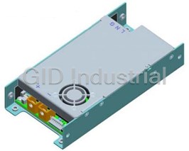
400W, 24V, UNIVERSAL AC INPUT FRONT END, TOP SIDE FAN
400 W, Single Output, 24 VDC@16.7 A Open Frame AC-DC Power Supply
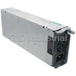
850 W, Single Output, 12 VDC@71 A Enclosed AC-DC Power Supply
850 W, Single Output, 12 VDC@71 A Enclosed AC-DC Power Supply
850W, 12V, UNIVERSAL AC INPUT FRONT END, CLASS A EMI
850 W, Single Output, 12 VDC@71 A Enclosed AC-DC Power Supply
Request a Quote

The quote request has been received
Close

Facing challenges or have inquiries? Feel free to contact us!
Call Us +1-469-283-2440
What they say about us
FANTASTIC RESOURCE
One of our top priorities is maintaining our business with precision, and we are constantly looking for affiliates that can help us achieve our goal. With the aid of GID Industrial, our obsolete product management has never been more efficient. They have been a great resource to our company, and have quickly become a go-to supplier on our list!
Bucher Emhart Glass
EXCELLENT SERVICE
With our strict fundamentals and high expectations, we were surprised when we came across GID Industrial and their competitive pricing. When we approached them with our issue, they were incredibly confident in being able to provide us with a seamless solution at the best price for us. GID Industrial quickly understood our needs and provided us with excellent service, as well as fully tested product to ensure what we received would be the right fit for our company.
Fuji
HARD TO FIND A BETTER PROVIDER
Our company provides services to aid in the manufacture of technological products, such as semiconductors and flat panel displays, and often searching for distributors of obsolete product we require can waste time and money. Finding GID Industrial proved to be a great asset to our company, with cost effective solutions and superior knowledge on all of their materials, it’d be hard to find a better provider of obsolete or hard to find products.
Applied Materials
CONSISTENTLY DELIVERS QUALITY SOLUTIONS
Over the years, the equipment used in our company becomes discontinued, but they’re still of great use to us and our customers. Once these products are no longer available through the manufacturer, finding a reliable, quick supplier is a necessity, and luckily for us, GID Industrial has provided the most trustworthy, quality solutions to our obsolete component needs.
Nidec Vamco
TERRIFIC RESOURCE
This company has been a terrific help to us (I work for Trican Well Service) in sourcing the Micron Ram Memory we needed for our Siemens computers. Great service! And great pricing! I know when the product is shipping and when it will arrive, all the way through the ordering process.
Trican Well Service
GO TO SOURCE
When I can't find an obsolete part, I first call GID and they'll come up with my parts every time. Great customer service and follow up as well. Scott emails me from time to time to touch base and see if we're having trouble finding something.....which is often with our 25 yr old equipment.
ConAgra Foods