

 Manufacturers
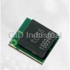
LITTELFUSE, INC. ZEN056V130A24LS
Description
ESD Suppressor Polymer 3-Pin T/R
ZEN056V130A24LS
Part Number
ZEN056V130A24LS
Price
Request Quote
Manufacturer
LITTELFUSE, INC.
Lead Time
Request Quote
Category
Circuit Protection » ESD Suppressors
Specifications
Manufacturer
Littelfuse, Inc.
Manufacturers Part #
ZEN056V130A24LS
Industry Aliases
ZEN056V130A24LS, RF1489-000
Sub-Category
ESD Suppressors
Packaging
Tape and Reel
Factory Pack Quantity
3000
Datasheet

Extracted Text
POLYZEN DEVICES Polymer Protected Zener Diode PolyZen devices are polymer-enhanced, precision Zener diodes. They offer resettable protection against multi-Watt fault events without the need for multi-Watt heat sinks. The Zener diode used for voltage clamping a PolyZen device was selected due to its relatively flat voltage vs. current response. This helps improve output voltage clamping, even when input voltage is high and diode currents are large. An advanced feature of the PolyZen device is that the Zener diode is thermally coupled to a resistively non- linear, PPTC (polymer positive temperature coefficient) layer. This PPTC layer is fully integrated into the device and is electrically in series between V and the diode IN clamped V . OUT This advanced PPTC layer responds to either extended diode heating or overcurrent events by transitioning from a low to high resistance state, also known as “tripping.” A tripped PPTC will limit current and generate voltage drop. It helps to protect both the Zener diode and the follow-on electronics and effectively increases the diode’s power handling capability. The polymer-enhanced Zener diode helps protect sensitive portable electronics from damage caused by inductive voltage spikes, voltage transients, incorrect power supplies and reverse bias. These devices are particularly suitable for portable electronics and other low-power DC devices. BENEFITS APPLICATIONS • Stable Zener diode helps shield downstream • DC power port protection in portable electronics electronics from overvoltage and reverse bias • DC power port protection for systems using barrel • Trip events shut out overvoltage and reverse bias jacks for power input sources • Internal overvoltage and transient suppression • Analog nature of trip events helps minimize damage • DC output voltage regulation from upstream inductive spikes • Tablet PCs and portable electronics • Minimal power dissipation requirements • Single component placement FEATURES • Overvoltage transient suppression • Multi-Watt power handling capability • Integrated device construction • Stable V vs. fault current Z • Time delayed, overvoltage trip • RoHS compliant • Time delayed, reverse bias trip • Halogen free ≥ ≥ ≥ (refers to: Br 900ppm, Cl 900ppm, Br+Cl 1500ppm) RoHS Compliant, ELV Compliant Specifications subject to change without notice. ©2016 Littelfuse, Inc. 27 PolyZen Devices Polymer Protected Zener Diode Figure PZ1 — Typical Application Block Diagram Power Supply (External or Internal) Protected Electronics GND 2 V IN PolyZen 1 Device + V OUT 3 R Regulated LOAD Output Protected Downstream Electronics Table PZ1 — Electrical Characteristics (Performance ratings @ 25°C unless otherwise specified) V (V) V I Z INT MAX FLT MAX I Test Test HOLD I @ 20°C R R V Current I Voltage Zt Typ 1MAX INT MAX FLT MAX Part Number Min Typ Max (A) (A) (Ω) (Ω) (V) (A) (A) (V) ZEN056V130A24LS 5.45 5.60 5.75 0.10 1.30 0.12 0.16 24 3 +10/-40 +24/-16 † ZEN059V130A24LS 5.80 5.90 6.00 0.10 1.30 0.12 0.15 24 3 +6/-40 +24/-16 ZEN065V130A24LS 6.35 6.50 6.65 0.10 1.30 0.12 0.16 24 3 +6/-40 +24/-16 ZEN098V130A24LS 9.60 9.80 10.00 0.10 1.30 0.12 0.16 24 3 +3.5/-40 +24/-16 ZEN132V130A24LS 13.20 13.40 13.60 0.10 1.30 0.12 0.16 24 3 +2/-40 +24/-16 ZEN164V130A24LS 16.10 16.40 16.60 0.10 1.30 0.12 0.16 24 3 +1.25/-40 +24/-16 ZEN056V230A16LS 5.45 5.60 5.75 0.10 2.30 0.04 0.06 16 5 +5/-40 +16/-12 ZEN065V230A16LS 6.35 6.50 6.65 0.10 2.30 0.04 0.06 16 5 +3.5/-40 +16/-12 ZEN098V230A16LS 9.60 9.80 10.00 0.10 2.30 0.04 0.06 16 5 +3.5/-40 +16/-12 ZEN132V230A16LS 13.20 13.40 13.60 0.10 2.30 0.04 0.06 16 5 +2/-40 +20/-12 ZEN056V075A48LS 5.45 5.60 5.75 0.10 0.75 0.28 0.45 48 3 +10/-40 +48/-16 ZEN132V075A48LS 13.20 13.40 13.60 0.10 0.75 0.28 0.45 48 3 +2/-40 +48/-16 ZEN056V115A24LS 5.45 5.60 5.75 0.10 1.15 0.15 0.18 24 3 +10/-40 +24/-16 NEW ZEN056V130A16YM 5.35 5.60 5.85 0.10 1.30 0.110 0.160 14 3 +3/-40 +16/-12 NEW ZEN056V175A12YM 5.35 5.60 5.85 0.10 1.75 0.050 0.095 12 4 +3/-40 +12/-12 NEW ZEN132V130A16YM 13.20 13.40 13.80 0.10 1.30 0.110 0.160 14 3 +1/-40 +20/-12 NEW ZEN132V175A12YM 13.20 13.40 13.80 0.10 1.75 0.050 0.095 12 4 +1/-40 +20/-12 NEW ZEN056V130A24YC 5.35 5.60 5.85 0.10 1.30 0.110 0.170 24 3 +4/-40 +24/-16 NEW ZEN056V230A16YC 5.35 5.60 5.85 0.10 2.30 0.040 0.070 16 5 +3/-40 +16/-12 NEW ZEN056V260A16YC 5.35 5.60 5.85 0.10 2.60 0.040 0.055 16 5 +3/-40 +16/-12 NEW ZEN132V130A24YC 13.20 13.40 13.80 0.10 1.30 0.110 0.170 24 3 +1/-40 +24/-16 NEW ZEN132V230A16YC 13.20 13.40 13.80 0.10 2.30 0.040 0.070 16 5 +1/-40 +20/-12 NEW ZEN132V260A16YC 13.20 13.40 13.80 0.10 2.60 0.040 0.055 16 5 +1/-40 +20/-12 LS module height is 1.7mm typical. YM module height is 1.2mm typical. YC module Table PZ2 — Definition of Terms V Zener clamping voltage measured at current I and 20°C. Z ZT Polymer PTC I Test current at which V is measured. ZT Z V IN I Maximum steady state current I that will not generate a trip event at the specified temperature. HOLD PTC V OUT Ratings assume I = 0A. FLT Zener R Typical resistance between V and V pins when the device is at room temperature. Diode Typ IN OUT R The maximum resistance between V and V pins, at room temperature, one hour after first trip or 1MAX IN OUT after reflow soldering. GND I Current flowing through the Zener diode. FLT I Maximum RMS fault current the Zener diode component of the device can withstand and remain resettable; FLT MAX I I testing is conducted at rated voltage with no load connected to V . PTC OUT OUT V The voltage (V - V “post trip”) at which typical qualification devices (98% devices, 95% confidence) survived INT MAX IN OUT V IN at least 100 trip cycles and 24 hours trip endurance when “tripped” at the specified voltage and current (I ). PTC V OUT I Current flowing through the PPTC portion of the circuit. PTC I Current flowing out the V pin of the device. OUT OUT I FLT Trip Event A condition where the PPTC transitions to a high resistance state, thereby limiting I , and significantly PTC increasing the voltage drop between V and V . IN OUT GND RoHS Compliant, ELV Compliant 28 Specifications subject to change without notice. ©2016 Littelfuse, Inc. PolyZen Devices Polymer Protected Zener Diode Figures PZ2-PZ9 — Typical Performance Curves for PolyZen Devices - LS Series V V Peak vs. Peak vs. II RMS (I RMS (I = 0) = 0) Ti Ti me-to-T me-to-T rip vs. rip vs. II RMS (I RMS (I = 0) = 0) Figure PZ2 Figure PZ3 OUT OUT FL FL TT OUT OUT FL FL TT OUT OUT Time-to-Trip vs. I RMS (I = 0) V V Peak vs. Peak vs. II RMS (I RMS (I = 0) = 0) Time-to-Trip vs. I RMS (I = 0) FLT OUT OUT OUT FL FL TT OUT OUT FLT OUT 22.0 22.0 10 10 22.0 A A = ZEN056V1yyA24LS = ZEN056V1yyA24LS 10 A A = ZEN056V1yyA24LS = ZEN056V1yyA24LS 22.0 10 20.0 20.0 FF A = ZEN056V1yyA24LS A = ZEN056V1yyA24LS A = ZEN056V1yyA24LS A = ZEN056V1yyA24LS B B = ZEN059V130A24LS = ZEN059V130A24LS B B = ZEN059V130A24LS = ZEN059V130A24LS 20.0 20.0 18.0 18.0 FF B = ZEN059V130A24LS B = ZEN059V130A24LS B = ZEN059V130A24LS B = ZEN059V130A24LS C C = ZEN065V130A24LS = ZEN065V130A24LS C C = ZEN065V130A24LS = ZEN065V130A24LS 18.0 18.0 C = ZEN065V130A24LS C = ZEN065V130A24LS 16.0 16.0 C = ZEN065V130A24LS C = ZEN065V130A24LS D D = ZEN098V130A24LS = ZEN098V130A24LS D D = ZEN098V130A24LS = ZEN098V130A24LS EE 16.0 16.0 D = ZEN098V130A24LS 11 D = ZEN098V130A24LS E D = ZEN098V130A24LS D = ZEN098V130A24LS E E E = ZEN132V130A24LS = ZEN132V130A24LS E E = ZEN132V130A24L = ZEN132V130A24L SS 14.0 14.0 1 1 E = ZEN132V130A24LS E = ZEN132V130A24LS E = ZEN132V130A24LS E = ZEN132V130A24LS 14.0 14.0 F F = ZEN164V130A24LS = ZEN164V130A24LS F F = ZEN164V130A24L = ZEN164V130A24L SS 12.0 12.0 D D F = ZEN164V130A24LS F = ZEN164V130A24LS F = ZEN164V130A24LS F = ZEN164V130A24LS 12.0 12.0 10.0 10.0 D D FF 10.0 10.0 8.0 8.0 FF CC A A 0.1 0.1 BB 8.0 8.0 CC EE 6.0 6.0 0.1 B A A 0.1 CC BB B D D E E 6.0 6.0 A A CC BB D D 4.0 4.0 A A 4.0 4.0 2.0 2.0 2.0 2.0 00 0.01 0.01 01 01 23 23 45 45 67 67 89 89 10 10 01 01 23 23 45 45 67 67 89 89 10 10 00 0.01 0.01 01 01 23 23 45 45 67 67 89 89 10 10 01 01 23 23 45 45 67 67 89 89 10 10 I I RMS (A) RMS (A) I I RMS (A) RMS (A) FL FL TT FL FL TT I RMS (A) I RMS (A) I RMS (A) I RMS (A) FLT FLT FLT FLT Figure PZ4 Figure PZ5 V V Peak vs. Peak vs. II RMS (I RMS (I = 0) = 0) Ti Ti me-to-T me-to-T rip vs. rip vs. II RMS (I RMS (I = 0) = 0) OUT OUT FL FL TT OUT OUT FL FL TT OUT OUT V V Peak vs. Peak vs. II RMS (I RMS (I = 0) = 0) Ti Ti me-to-T me-to-T rip vs. rip vs. II RMS (I RMS (I = 0) = 0) OUT OUT FL FL TT OUT OUT FL FL TT OUT OUT 22.0 22.0 100 100 22.0 A = ZEN056V230A16LS A = ZEN056V230A16LS A = ZEN056V230A16LS A = ZEN056V230A16LS 22.0 100 100 20.0 20.0 A = ZEN056V230A16LS A = ZEN056V230A16LS A = ZEN056V230A16LS A = ZEN056V230A16LS B = ZEN065V230A16LS B = ZEN065V230A16LS B = ZEN065V230A16LS B = ZEN065V230A16LS 20.0 20.0 18.0 18.0 B = ZEN065V230A16LS B = ZEN065V230A16LS B = ZEN065V230A16LS B = ZEN065V230A16LS C = ZEN098V230A16LS C = ZEN098V230A16LS C = ZEN098V230A16LS C = ZEN098V230A16LS D D 18.0 18.0 10 10 16.0 16.0 C = ZEN098V230A16LS C = ZEN098V230A16LS C = ZEN098V230A16LS C = ZEN098V230A16LS D = ZEN132V230A16LS D = ZEN132V230A16LS D = ZEN132V230A16LS D = ZEN132V230A16LS D D 10 10 16.0 16.0 D = ZEN132V230A16LS D = ZEN132V230A16LS D = ZEN132V230A16LS D = ZEN132V230A16LS 14.0 14.0 14.0 14.0 12.0 12.0 CC 11 12.0 12.0 C 10.0 10.0 C 11 10.0 10.0 8.0 8.0 BB 8.0 8.0 BB A A 6.0 6.0 B B 0.1 0.1 A BB A A A D D CC 6.0 6.0 0.1 0.1 4.0 4.0 A A D D C C 4.0 4.0 2.0 2.0 2.0 2.0 0.01 0.01 00 0.01 0 01 01 23 23 45 45 67 67 89 89 10 10 0.0101 01 23 23 45 45 67 67 89 89 10 10 0 01 23 45 67 89 10 01 23 45 67 89 10 01 23 45 67 89 10 01 23 45 67 89 10 V Peak vs. I RMS (I = 0) Ti Ti me-to-T me-to-T rip vs. rip vs. I I RMS (I RMS (I = 0) = 0) V Peak vs. I RMS (I = 0) OUT I I RMS (A) RMS (A) FLT OUT I I RMS (A) RMS (A) FL FL TT OUT OUT OUT FLT OUT FL FL TT FL FL TT II RMS (A) RMS (A) II RMS (A) RMS (A) 0.0 0.0 FL FL TT 100 FL FL TT 100 A A = ZENxxxV1yyA24LS = ZENxxxV1yyA24LS A A = ZENxxxV1yyA24LS = ZENxxxV1yyA24LS Figure PZ6 Figure PZ7 VV Peak vs. Peak vs. I I RMS (I RMS (I B B = ZENxxxV230A16LS = ZENxxxV230A16LS = 0) = 0) Ti Ti me-to-T me-to-T rip vs. rip vs. I I RMS (I RMS (I B B = ZENxxxV230A16LS = ZENxxxV230A16LS = 0) = 0) OUT OUT FL FL TT OUT OUT FL FL TT OUT OUT -0.2 -0.2 10 10 C C = ZENxxxV075A48LS = ZENxxxV075A48LS C C = ZENxxxV075A48LS = ZENxxxV075A48LS 0.0 0.0 100 100 A A = ZENxxxV1yyA24LS = ZENxxxV1yyA24LS A A = ZENxxxV1yyA24LS = ZENxxxV1yyA24LS -0.4 -0.4 B B = ZENxxxV230A16LS = ZENxxxV230A16LS B B = ZENxxxV230A16LS = ZENxxxV230A16LS 1 -0.2 -0.2 1 10 10 C C = ZENxxxV075A48LS = ZENxxxV075A48LS C C = ZENxxxV075A48LS = ZENxxxV075A48LS -0.6 -0.6 -0.4 -0.4 0.1 0.1 1 1 -0.8 -0.8 -0.6 -0.6 BB 0.01 0.01 -1.0 -1.0 0.1 0.1 A A AA -0.8 -0.8 B B C C C C -1.2 -1.2 0.001 0.001 BB 0.01 0.01 -50 -50 -40 -40 -30 -30 -20 -20 -10 -10 00 -50 -50 -40 -40 -30 -30 -20 -20 -10 -10 00 -1.0 -1.0 AA AA I I RMS (A) RMS (A) I I RMS (A) RMS (A) FL FL T T FL FL T T BB CC CC -1.2 -1.2 0.001 0.001 -50 -50 -40 -40 -30 -30 -20 -20 -10 -10 0 0 -50 -50 -40 -40 -30 -30 -20 -20 -10 -10 0 0 I I RMS (A) RMS (A) I I RMS (A) RMS (A) FL FL T T FL FL T T Figure PZ8 Figure PZ9 TT emperature Effect on emperature Effect on I I (I (I = 0) = 0) Ti Ti me-to-T me-to-T rip vs. rip vs. I I RMS (I RMS (I = 0) = 0) HOLD HOLD FL FL TT PTC PTC FL FL TT 10 3.5 3.5 10 A A = ZENxxxV130A24LS = ZENxxxV130A24LS A A = ZENxxxV1yyA24LS = ZENxxxV1yyA24LS TT emperature Effect on emperature Effect on I I (I (I = 0) = 0) Ti Ti me-to-T me-to-T rip vs. rip vs. I I RMS (I RMS (I = 0) = 0) HOLD HOLD FL FL TT PTC PTC FL FL TT 3.0 3.0 B B = ZENxxxV230A16LS = ZENxxxV230A16LS B B = ZENxxxV230A16LS = ZENxxxV230A16LS BB C C = ZENxxxV075A48LS = ZENxxxV075A48LS C C = ZENxxxV075A48LS = ZENxxxV075A48LS 10 10 3.5 3.5 11 2.5 2.5 A A = ZENxxxV130A24LS = ZENxxxV130A24LS A A = ZENxxxV1yyA24LS = ZENxxxV1yyA24LS D D = ZENxxxV115A24LS = ZENxxxV115A24LS 3.0 3.0 B B = ZENxxxV230A16LS = ZENxxxV230A16LS B B = ZENxxxV230A16LS = ZENxxxV230A16LS BB 2.0 2.0 A A C C = ZENxxxV075A48LS = ZENxxxV075A48LS C C = ZENxxxV075A48LS = ZENxxxV075A48LS 1 1 0.1 0.1 2.5 2.5 D D = ZENxxxV115A24LS = ZENxxxV115A24LS 1.5 1.5 D D 2.0 2.0 AA 1.0 1.0 0.1 0.1 C 0.01 0.01 C BB 1.5 1.5 DD 0.5 0.5 AA CC 1.0 1.0 CC 0.01 0.01 0.0 0.0 0.001 0.001 BB -40 -40 -20 -20 02 02 04 04 06 06 08 08 00 100 100 05 05 10 10 15 15 20 20 25 25 30 30 35 35 40 40 45 45 0.5 0.5 Ambient Ambient Te Te mperature (˚C) mperature (˚C) AA I I RMS (A) RMS (A) PTC PTC CC 0.0 0.0 0.001 0.001 -40 -40 -20 -20 02 02 04 04 06 06 08 08 0 0 100 100 05 05 10 10 15 15 20 20 25 25 30 30 35 35 40 40 45 45 Ambient Ambient Te Te mperature (˚C) mperature (˚C) I I RMS (A) RMS (A) PTC PTC RoHS Compliant, ELV Compliant Specifications subject to change without notice. ©2016 Littelfuse, Inc. 29 I (A) I (A) V Peak (V) V Peak (V) HOLD HOLD V Peak (V) OUT OUT V Peak (V) V V Peak (V) Peak (V) I (A)I (A) V Peak (V) V Peak (V) OUT HOLD HOLD VOUT V Peak (V) Peak (V) OUT OUT OUT OUT V V Peak (V) Peak (V) OUT OUT OUT OUT Time-to-T T rip (s) ime-to-Trip (s) Time-to-T T rip (s) ime-to-Trip (s) Time-to-T Time-to-T rip (s) rip (s) Time-to-T Time-to-T rip (s) rip (s) Time-to-T T rip (s) ime-to-Trip (s) Time-to-T T rip (s) ime-to-Trip (s) Time-to-T Time-to-T rip (s) rip (s) Time-to-T Time-to-T rip (s) rip (s) PolyZen Devices Polymer Protected Zener Diode Figures PZ10-PZ15 — Typical Performance Curves for PolyZen Devices - YM Series V Peak vs. I RMS (I = 0) Time-to-Trip vs. I RMS (I = 0) OUT FLT OUT FLT OUT Figure PZ10 Figure PZ11 V Peak vs. I RMS (I = 0) Time-to-Trip vs. I RMS (I = 0) 18.0 100 OUT FLT OUT FLT OUT 18.0 B C A = ZEN056V1yyAzzYM 100 A = ZEN056V130A16YM 16.0 B = ZEN132V130A16YM B = ZEN056V175A12YM B C A = ZEN056V1yyAzzYM A = ZEN056V130A16YM 16.0 14.0 C = ZEN132V175A12YM C = ZEN132V130A16YM 10 B = ZEN132V130A16YM B = ZEN056V175A12YM 14.0 D = ZEN132V175A12YM 12.0 C = ZEN132V175A12YM C = ZEN132V130A16YM 10 D = ZEN132V175A12YM 12.0 10.0 1 10.0 8.0 1 8.0 6.0 A B 6.0 A 0.1 4.0 A C B 4.0 0.1 A 2.0 C D 2.0 0.0 D 0.01 01 23 4 56 78 0.0 0.5 1.01.5 2.0 2.5 3.0 3.5 4.0 0.0 0.01 01 23 4 56 78 I RMS (A) FLT 0.0 0.5 1.01.5 2.0 2.5 3.0 3.5 4.0 I RMS (A) FLT I RMS (A) FLT I RMS (A) FLT Figure PZ12 Figure PZ13 V Peak vs. I RMS (I = 0) Time-to-Trip vs. I RMS (I = 0) OUT FLT OUT FLT OUT 0.0 V Peak vs. I RMS (I = 0) 100 Time-to-Trip vs. I RMS (I = 0) OUT FLT OUT FLT OUT C 0.0 A = ZEN056V130A16YM 100 A = ZEN056V130A16YM -0.2 C B = ZENxxxV1yyAzzYM B = ZEN132V130A16YM B A = ZEN056V130A16YM A = ZEN056V130A16YM -0.4 -0.2 10 C = ZENxxxV175A12YM B = ZENxxxV1yyAzzYM B = ZEN132V130A16YM B -0.4 10 -0.6 C = ZENxxxV175A12YM B -0.6 -0.8 1 B A -0.8 -1.0 1 A -1.0 -1.2 0.1 -1.2 0.1 -1.4 A -1.4 -1.6 0.01 A -1.6 -1.8 0.01 -1.8 -2.0 0.001 -40 -30 -20 -100 -40 -30 -20 -100 -2.0 0.001 -40 -30 -20 -100 -40 -30 -20 -100 I RMS (A) I RMS (A) FLT FLT I RMS (A) I RMS (A) FLT FLT Figure PZ14 Figure PZ15 Temperature Effect on I (I = 0) HOLD FLT Time-to-Trip vs. I RMS (I = 0) PTC FLT 3 100 B A = ZENxxxV130A16YM A = ZENxxxV130A16YM 2.5 B = ZENxxxV175A12YM B = ZENxxxV175A12YM Temperature Effect on I (I = 0) 10 HOLD FLT Time-to-Trip vs. I RMS (I = 0) PTC FLT A 3 100 2 B A = ZENxxxV130A16YM 1 A = ZENxxxV130A16YM 2.5 B = ZENxxxV175A12YM B = ZENxxxV175A12YM 1.5 10 A 0.1 2 1 A 1 B 0.01 1.5 0.5 0.1 1 A 0.001 0 02 10 0 30 40 -40 -20 020406080100 B 0.01 0.5 I RMS (A) PTC Ambient Temperature (°C) 0.001 0 02 10 0 30 40 -40 -20 020406080100 V Peak vs. I RMS (I = 0) Time-to-Trip vs. I RMS (I = 0) OUT FLT OUT FLT OUT I RMS (A) Ambient Temperature (°C) PTC Figures PZ16-PZ21 — Typical Performance Curves for PolyZen Devices - YC Series 18.0 100 B A = ZEN056VyyyAzzYC A = ZEN056V130A24YC 16.0 C B = ZEN132V130A24YC B = ZEN132V130A24YC Figure PZ16 Figure PZ17 V Peak vs. I RMS (I = 0) Time-to-Trip vs. I RMS (I = 0) OUT FLT OUT 14.0 FLT OUT C = ZEN132V2yyA16YC C = ZEN056V2yyA16YC 10 18.0 100 D = ZEN132V2yyA16YC 12.0 B A = ZEN056VyyyAzzYC A = ZEN056V130A24YC 16.0 10.0 C B = ZEN132V130A24YC B = ZEN132V130A24YC 1 14.0 C = ZEN132V2yyA16YC A C = ZEN056V2yyA16YC 10 D 8.0 D = ZEN132V2yyA16YC 12.0 A B C 6.0 10.0 0.1 4.0 1 A D 8.0 2.0 A B C 6.0 0.0 0.01 0.1 0.0 0.5 1.01.5 2.0 2.5 3.0 3.5 4.0 01 23 45 67 8 4.0 I RMS (A) I RMS (A) FLT FLT 2.0 0.0 0.01 0.0 0.5 1.01.5 2.0 2.5 3.0 3.5 4.0 01 23 45 67 8 I RMS (A) I RMS (A) FLT FLT RoHS Compliant, ELV Compliant 30 Specifications subject to change without notice. ©2016 Littelfuse, Inc. V Peak (V) V Peak (V) OUT OUT V V Peak (V) Peak (V) OUT OUT V V Peak (V) Peak (V) OUT OUT I (A) I (A) HOLD HOLD Time-to-Trip (s) Time-to-Trip (s) Time-to-Trip (s) Time-to-Trip (s) Time-t Time-t o-Tro-T ip (s) rip (s) Time-t Time-t o-Tro-T ip (s) rip (s) PolyZen Devices Polymer Protected Zener Diode (Cont’d) Figures PZ16-PZ21 — Typical Performance Curves for PolyZen Devices - YC Series Figure PZ18 Figure PZ19 V Peak vs. I RMS (I = 0) Time-to-Trip vs. I RMS (I = 0) OUT FLT OUT FLT OUT 100 0.0 D A = ZEN056V130A24YC A = ZEN056V130A24YC C -0.2 B = ZEN056V2yyA16YC 10 B = ZEN056V2yyA16YC C = ZEN132V130A24YC C = ZEN132V130A24YC D = ZEN132V2yyA16YC -0.4 D = ZEN132V2yyA16YC 1 B -0.6 C 0.1 -0.8 D -1.0 0.01 B A A -1.2 -40 -30 -20 -100 0.001 -40 -30 -20 -100 I RMS (A) FLT I RMS (A) FLT Figure PZ20 Figure PZ21 Time-to-Trip vs. I RMS (I = 0) Temperature Effect on I (I = 0) PTC FLT HOLD FLT 100 4 B A = ZENxxxV130A24YC A = ZENxxxV130A24YC 3.5 B = ZENxxxV2yyA16YC B = ZENxxxV230A16YC 10 A 3 C = ZENxxxV260A16YC 2.5 1 2 C 0.1 1.5 1 B 0.01 A 0.5 0 0.001 -40 -20 020406080100 010203040 Ambient Temperature (°C) I RMS (A) PTC Table PZ3 — General Characteristics for PolyZen Devices Operating temperature range -40° to +85°C Storage temperature -40° to +85°C ESD withstand 15kV Human body model Diode capacitance 4200pF Typical @ 1MHz, 1V RMS Construction RoHS compliant Figures PZ22-PZ34 — Basic Operation Examples for PolyZen Devices - LS Series Figure PZ22 Hot-Plug Response ZEN056V130A24LS vs. a 22V/120W Universal Power Supply 350 35 C A = V IN Capacitive B = V 300 30 Current Spike OUT Supply Voltage C = CURRENT (I ) Supply Voltage FLT Returns to Normal Dropped by Current Current Pulled to D = POWER 250 25 GND via Diode A 200 20 D 15 150 PPTC Switches to Output Voltage High Resistance Remains Clamped 10 100 A B B 5 50 V Peak D OUT C 0 0 0 0.01 0.02 0.03 0.04 0.05 0.06 0.07 0.08 Time (s) RoHS Compliant, ELV Compliant Specifications subject to change without notice. ©2016 Littelfuse, Inc. 31 V Peak (V) OUT I (A) HOLD Voltage (V) and Current (A) Time-to-Trip (s) Time-to-Trip (s) Power (Watts) PolyZen Devices Typical Fault Response: ZEN056V1xxA24L Typical Fault Response: ZEN056V1xxA24L S S Typical Fault Response: ZEN059V130A24LS Typical Fault Response: ZEN059V130A24LS 20V20V , 3.5A Current Limited Source (I , 3.5A Current Limited Source (I=0) =0) 24V24V , 6A Current Limited Source (I , 6A Current Limited Source (I=0) =0) Polymer Protected Zener Diode OUT OUT OUT OUT 20 20 24 24 A A A A A = V Ty (V pical Fault Response: ZEN056V1xxA24L Ty ) pical Fault Response: ZEN056V1xxA24L S S A = Ty V pical Fault Response: ZEN059V130A24LS (V Ty ) pical Fault Response: ZEN059V130A24LS A = V (V)IN A = V (V)IN IN 22 22 IN 18 18 B = V20V (V20V , 3.5A Current Limited Source (I ) , 3.5A Current Limited Source (I=0) =0) B = V 24V (V24V ), 6A Current Limited Source (I , 6A Current Limited Source (I=0) =0) B = V (V OUT ) OUT OUT B = V (V OUT ) OUT OUT OUT 20 20 OUT 16 16 20 20 24 24 (Cont’d) Figures PZ22-PZ34 — Basic Operation Examples for PolyZen Devices - LS Series C = I (A) C = I (A) C = I (AFL ) T 18C = I (AFL ) T FLT A A 18 FLT A A A = V A = (VV ) (V) A = V A = (VV ) (V) IN IN 22 22 IN IN 14 14 18 18 16 Typical Fault Response: ZEN056V1xxA24L Typical Fault Response: ZEN056V1xxA24L S S 16 Typical Fault Response: ZEN059V130A24LS Typical Fault Response: ZEN059V130A24LS B = V B = (V V ) (V) B = V B = (V V ) (V) OUT OUT 20 20 OUT OUT 12 12 16 16 14 20V20V , 3.5A Current Limited Source (I , 3.5A Current Limited Source (I=0) =0) 14 24V24V , 6A Current Limited Source (I , 6A Current Limited Source (I=0) =0) OUT OUT OUT OUT C = IC = (A I ) (A) C = IC = (A I ) (A) FLT FLT 18 18 FLT FLT Figure PZ23 Figure PZ24 20 20 24 24 10 12 10 12 14 14 A A A A Typical Fault Response: ZEN056V1xxA24L Typical Fault Response: ZEN056V1xxA24L S S Typical Fault Response: ZEN059V130A24LS Typical Fault Response: ZEN059V130A24LS 16 16 A = V A = (VV ) (V) A = V A = (VV ) (V) IN IN 22 22 IN IN 18 18 10 10 8 8 12 12 20V20V , 3.5A Current Limited Source (I , 3.5A Current Limited Source (I=0)=0) 24V24V , 6A Current Limited Source (I , 6A Current Limited Source (I=0)=0) OUT OUT OUT OUT 14 14 B = V B = (V V ) (V) B = V B = (V V ) (V) OUT OUT 20 20 OUT OUT 8 8 20 20 B 24 24 16 16 B 6 6 B 10 10 12 12 B C = IC = (A I ) (A) A A C = IC = (A I ) (A) A A FLT FLT 18 18 FLT FLT A = V A IN= (V V)IN (V) 6 6A = V A IN= (V V)IN (V) 22 22 18 18 14 14 4 10 10 4 8 8 16 16 B = V B OUT = (V VOUT ) (V) 4 4B = V B OUT = (V VOUT ) (V) 20 20 16 16 12 12 8 8 B B 2 14 14 6 2 6 C = IC FLT= (A IFL ) T (A) 2 2C = IC FLT= (A IFL ) T (A) B B 18 18 C C C 6 6 C 14 14 10 10 12 12 0 0 0 0 4 4 16 16 4 4 -0.02 0.02 0.06 0.10 0.14 0.18 0.02 0.05 0.10 0.15 -0.02 0.02 0.06 0.10 0.14 0.18 10 0.02 10 0.05 0.10 0.15 12 12 8 8 14 14 2 2 2 2 Time (s) Time (s) 8 8 Time (s) Time (s) B B 10 10 C C 12 12 C C 6 6 B B 0 0 0 0 6 6 10 10 8-0.028-0.02 0.02 0.02 0.06 0.06 0.10 0.10 0.14 0.14 0.18 0.18 0.02 0.02 0.05 0.05 0.10 0.10 0.15 0.15 4 4 4 4 8 8 B B Time (s) Time (s) Time (s) Time (s) 6 6 B B 2 2 2 2 6 6 C C C C 4 4 0 0 0 0 4 4 -0.02-0.02 0.02 0.02 0.06 0.06 0.10 0.10 0.14 0.14 0.18 0.18 0.02 0.02 0.05 0.05 0.10 0.10 0.15 0.15 Typical Fault Response: ZEN065V130A24L Typical Fault Response: ZEN065V130A24L S S Typical Fault Response: ZEN098V130A24LS Typical Fault Response: ZEN098V130A24LS 2 2 2 2 24V24V , 5.0A Current Limited Source (I , 5.0A Current Limited Source (I=0) =0) 24V24V , 3.5A Current Limited Source (I , 3.5A Current Limited Source (I C =0)C =0) Time (s) Time (s) OUT OUTC C Time (s) Time (s) OUT OUT 0 0 0 0 26 24 26 24 -0.02-0.02 0.02 0.02 0.06 0.06 0.10 0.10 0.14 0.14 0.18 0.18 0.02 0.02 0.05 0.05 0.10 0.10 0.15 0.15 A A Typical Fault Response: ZEN065V130A24L Typical Fault Response: ZEN065V130A24L S S Typical Fault Response: ZEN098V130A24LS Typical Fault Response: ZEN098V130A24LS A = V (V) A = V (V) 24 24A = V (V)IN 22A = V (V)IN IN 22 IN Time (s) Time (s) A Time (s) Time (s) A 24V24V , 5.0A Current Limited Source (I , 5.0A Current Limited Source (I=0) =0) 24V24V , 3.5A Current Limited Source (I , 3.5A Current Limited Source (I=0) =0) OUT OUT OUT OUT 22 22 B = V (V) B = V (V) B = V (V OUT ) 20B = V (V OUT ) OUT 20 OUT 26 26 24 24 20 20 C = I (A) C = I (A) C = I (AFL ) T 18C = I (AFL ) T FLT 18 FLT A A Figure PZ25 Figure PZ26 24 24A = V A = (VV ) (V) A = V A = (VV ) (V) IN IN 22 22 IN IN 18 18 Typical Fault Response: ZEN065V130A24L Typical Fault Response: ZEN065V130A24L S S Typical Fault Response: ZEN098V130A24LS Typical Fault Response: ZEN098V130A24LS A A 16 16 22 22B = V B = (V V ) (V) B = V B = (V V ) (V) OUT OUT 20 20 OUT OUT 16 16 24V24V , 5.0A Current Limited Source (I , 5.0A Current Limited Source (I=0) =0) 24V24V , 3.5A Current Limited Source (I , 3.5A Current Limited Source (I=0) =0) OUT OUT 14 OUT OUT 14 20 20 C = IC = (A I ) (A) C = IC = (A I ) (A) 14 FLT FLT 18 18 FLT FLT 14 26 26 24 24 12 12 B B 18 18 Typical Fault Response: ZEN065V130A24L Typical Fault Response: ZEN065V130A24L S S Typical Fault Response: ZEN098V130A24LS Typical Fault Response: ZEN098V130A24LS A A 12 12 16 16 24 24A = V A = (VV ) (V) A = V A = (VV ) (V) IN IN 22 22 IN IN 10 24V24V , 5.0A Current Limited Source (I , 5.0A Current Limited Source (I=0)=0) 10 24V24V , 3.5A Current Limited Source (I , 3.5A Current Limited Source (I=0)=0) 16 16 OUT OUT A A OUT OUT 10 10 14 14 22 22B = V B = (V V ) (V) B = V B = (V V ) (V) OUT OUT 20 20 OUT OUT 26 26 24 24 8 14 14 8 B 8 8 B 20 20 12 12 A A C = IC = (A I ) (A) C = IC = (A I ) (A) B B FLT FLT 18 18 FLT FLT 12 24 12 24A = V A IN= (V V)IN (V) 22 22 6A = V A IN= (V V)IN (V) 6 6 6 18 18 A A 10 10 16 16 10 22 10 22 B = V B OUT = (V VOUT ) (V) 20 20 4B = V B OUT = (V VOUT ) (V) 4 4 4 16 16 8 8 20 20 B B 14 14 8 8 C = IC FLT= (A IFL ) T (A) 18 18 2C = IC FLT= (A IFL ) T (A) 2 2 2 14 14 C C C 6 6 C 18 6 18 6 12 12 B B 0 16 16 0 0 0 12 12 4 4 16 4 016 4 0 0.01 0.01 0.02 0.02 0.03 0.03 0.04 0.04 0.05 0.05 0.06 0.06 0.07 0.07 0.08 0.08 0.09 0.09 0.10 0.10 0 0 0.05 0.05 0.10 0.10 0.15 0.15 10 10 14 14 10 10 14 14 2 2 2 2 Time (s) Time (s) Time (s) 8 8 Time (s) B C C B 12 12 C C 8 8 B B 12 0 12 0 0 0 6 6 6 6 10 10 0 0 0.01 0.01 0.02 0.02 0.03 0.03 0.04 0.04 0.05 0.05 0.06 0.06 0.07 0.07 0.08 0.08 0.09 0.09 0.10 0.10 0 0 0.05 0.05 0.10 0.10 0.15 0.15 10 10 4 4 4 4 8 8 Time (s) Time (s) Time (s) Time (s) 8 8 B B 2 2 2 2 6 6 6 6 C C C C 0 0 0 0 4 4 4 4 0 0 0.01 0.01 0.02 0.02 0.03 0.03 0.04 0.04 0.05 0.05 0.06 0.06 0.07 0.07 0.08 0.08 0.09 0.09 0.10 0.10 0 0 0.05 0.05 0.10 0.10 0.15 0.15 2 2 2 2 Typical Fault Response: ZEN132V130A24L Typical Fault Response: ZEN132V130A24L S S Typical Fault Response: ZEN164V130A24LS Typical Fault Response: ZEN164V130A24LS Time (s) Time (s) C C Time (s) Time (s) C C 0 0 0 0 24V24V , 2.0A Current Limited Source (I , 2.0A Current Limited Source (I=0) =0) 24V24V , 1.0A Current Limited Source (I , 1.0A Current Limited Source (I=0) =0) OUT OUT OUT OUT 0 0 0.01 0.01 0.02 0.02 0.03 0.03 0.04 0.040.05 0.05 0.06 0.06 0.07 0.07 0.08 0.080.09 0.090.10 0.10 0 0 0.05 0.05 0.10 0.10 0.15 0.15 Figur 30e P 30 Z27 Figure P 30Z28 30 Time (s) Time (s) Time (s) Time (s) Typical Fault Response: ZEN132V130A24L Typical Fault Response: ZEN132V130A24L S S Typical Fault Response: ZEN164V130A24LS Typical Fault Response: ZEN164V130A24LS A = V (V) A = V (V) A = V (V)IN A = V (V)IN IN IN 24V24V , 2.0A Current Limited Source (I , 2.0A Current Limited Source (I=0) =0) 24V24V , 1.0A Current Limited Source (I , 1.0A Current Limited Source (I=0) =0) B = V (V) OUT OUT B = V (V) OUT OUT B = V (V OUT ) A B = V (V OUT ) 25 25 OUT A 25 25 OUT A A 30 30 30 30 C = I (A) C = I (A) C = I (AFL ) T C = I (AFL ) T FLT FLT A = V A = (VV ) (V) A = V A = (VV ) (V) IN IN IN IN Typical Fault Response: ZEN132V130A24L Typical Fault Response: ZEN132V130A24L S S Typical Fault Response: ZEN164V130A24LS Typical Fault Response: ZEN164V130A24LS 20 20 20 20 B B B = V B = (V V ) (V) B = V B = (V V ) (V) OUT OUT A A OUT OUT 25 25 25 25 A A 24V24V , 2.0A Current Limited Source (I , 2.0A Current Limited Source (I=0) =0) 24V24V , 1.0A Current Limited Source (I , 1.0A Current Limited Source (I=0) =0) OUT OUT OUT OUT C = IC = (A I ) (A) C = IC = (A I ) (A) FLT FLT FLT FLT B B 30 30 30 30 15 15 15 15 Typical Fault Response: ZEN132V130A24L Typical Fault Response: ZEN132V130A24L S S Typical Fault Response: ZEN164V130A24LS Typical Fault Response: ZEN164V130A24LS 20 20A = V A = (VV ) (V) 20 20A = V A = (VV ) (V) IN IN IN IN B B 24V24V , 2.0A Current Limited Source (I , 2.0A Current Limited Source (I=0)=0) 24V24V , 1.0A Current Limited Source (I , 1.0A Current Limited Source (I=0)=0) OUT OUT OUT OUT B = V B = (V V ) (V) B = V B = (V V ) (V) OUT OUT A A OUT OUT 25 25 25 25 A A 10 30 10 30 10 30 10 30 B B 15 15C = IC = (A I ) (A) 15 15C = IC = (A I ) (A) FLT FLT FLT FLT A = V A IN= (V V)IN (V) A = V A IN= (V V)IN (V) 20 20 20 20 B = V B OUT = (V VOUT ) (V) B = V B OUT = (V VOUT ) (V) B B 25 5 25 5 A A 25 5 25 5 A A 10 10 10 10 C = IC FLT= (A IFL ) T (A) C = IC FLT= (A IFL ) T (A) B B C C C C 15 15 15 15 20 0 20 0 20 0 20 0 B B 5 5 5 5 0 0 0.05 0.05 0.10 0.10 0.15 0.15 0.20 0.20 0.25 0.25 0.30 0.30 0.35 0.35 0.40 0.40 0.45 0.45 0.50 0.50 0 0 0.10 0.10 0.20 0.20 0.30 0.30 0.40 0.40 0.50 0.50 Time (s) B B Time (s) 10 10 Time (s) 10 10 Time (s) 15 15 C C 15 15 C C 0 0 0 0 0 0 0.05 0.05 0.10 0.10 0.15 0.15 0.20 0.20 0.25 0.25 0.30 0.30 0.35 0.35 0.40 0.40 0.45 0.45 0.50 0.50 0 0 0.10 0.10 0.20 0.20 0.30 0.30 0.40 0.40 0.50 0.50 5 5 5 5 10 10 10 10 Time (s) Time (s) Time (s) Time (s) C C C C 0 0 0 0 Figur5e P 5Z29 Figure P5Z30 5 0 0 0.05 0.05 0.10 0.10 0.15 0.15 0.20 0.20 0.25 0.25 0.30 0.30 0.35 0.35 0.40 0.40 0.45 0.45 0.50 0.50 0 0 0.10 0.10 0.20 0.20 0.30 0.30 0.40 0.40 0.50 0.50 Typical Fault Response: ZEN056V230A16LS Typical Fault Response: ZEN065V230A16LS Typical Fault Response: ZEN056V230A16LS Typical Fault Response: ZEN065V230A16LS Time (s) Time (s) C C Time (s) Time (s) C C 16V, 5.0A Current Limited Source (I =0) 16V, 3.5A Current Limited Source (I =0) 16V, 5.0A Current Limited Source (I =0) OUT 16V, 3.5A Current Limited Source (I =0) OUT OUT OUT 0 0 0 0 20 20 20 20 0 0 0.05 0.050.10 0.10 0.15 0.15 0.20 0.200.25 0.25 0.30 0.30 0.35 0.35 0.40 0.400.45 0.45 0.50 0.50 0 0 0.10 0.10 0.20 0.20 0.30 0.30 0.40 0.40 0.50 0.50 Typical Fault Response: ZEN056V230A16LS Typical Fault Response: ZEN056V230A16LS Typical Fault Response: ZEN065V230A16LS Typical Fault Response: ZEN065V230A16LS A = V A = (VV ) (V) A = V A = (VV ) (V) IN IN IN IN Time (s) Time (s) Time (s) Time (s) 16V16V , 5.0A Current Limited Source (I , 5.0A Current Limited Source (I=0) =0) 16V16V , 3.5A Current Limited Source (I , 3.5A Current Limited Source (I=0) =0) OUT OUT OUT OUT B = V B = (V V ) (V) A B = V B = (V V ) (V) OUT OUT A OUT OUT A A 20 20 20 20 15 15C = IC = (A I ) (A) 15 15C = IC = (A I ) (A) FLT FLT FLT FLT A = V A = (VV ) (V) A = V A = (VV ) (V) IN IN IN IN Typical Fault Response: ZEN056V230A16LS Typical Fault Response: ZEN056V230A16LS Typical Fault Response: ZEN065V230A16LS Typical Fault Response: ZEN065V230A16LS B = V B = (V V ) (V) A A B = V B = (V V ) (V) OUT OUT OUT OUT A A 16V16V , 5.0A Current Limited Source (I , 5.0A Current Limited Source (I=0) =0) 16V16V , 3.5A Current Limited Source (I , 3.5A Current Limited Source (I=0) =0) OUT OUT OUT OUT 15 15C = IC = (A I ) (A) 15 15C = IC = (A I ) (A) FLT FLT FLT FLT 20 20 20 20 10 10 10 10 Typical Fault Response: ZEN056V230A16LS Typical Fault Response: ZEN056V230A16LS Typical Fault Response: ZEN065V230A16LS Typical Fault Response: ZEN065V230A16LS A = V A = (VV ) (V) A = V A = (VV ) (V) IN IN IN IN 16V16V , 5.0A Current Limited Source (I , 5.0A Current Limited Source (I=0)=0) 16V16V , 3.5A Current Limited Source (I , 3.5A Current Limited Source (I=0)=0)B B OUT OUT OUT OUT B = V B = (V V ) (V) A A B = V B = (V V ) (V) OUT OUT OUT OUT A A 20 20 20 20 B B 10 10 10 10 15 15C = IC = (A I ) (A) 15 15C = IC = (A I ) (A) FLT FLT FLT FLT 5 5A = V A = (V V) (V) 5 5A = V A = (V V) (V) IN IN IN IN B B B = V B = (V V ) (V) A A B = V B = (V V ) (V) OUT OUT OUT OUT A A B B 15 15C = IC = (A I ) (A) 15 15C = IC = (A I ) (A) FLT FLT FLT FLT C C C 5 5 5 5 C 10 10 10 10 0 0 0 0 0 0 0.10 0.10 0.20 0.20 0.30 0.30 0 0 0.10 0.10 0.20 0.20 0.30 0.30 B B Time (s) Time (s) Time (s) Time (s) C B C B 10 10 10 10 C C 0 0 0 0 5 5 5 5 0 0 0.10 0.10 0.20 0.20 0.30 0.30 0 0 0.10 0.10 0.20 0.20 0.30 0.30 B B Time (s) Time (s) B B Time (s) Time (s) 5 5 5 5 C C RoHS Compliant, ELV Compliant 32 Specifications subject to change without notice. ©2016 Littelfuse, Inc. C C 0 0 0 0 0 0 0.10 0.10 0.20 0.20 0.30 0.30 0 0 0.10 0.10 0.20 0.20 0.30 0.30 Typical Fault Response: ZEN098V230A16L Typical Fault Response: ZEN098V230A16L S S Typical Fault Response: ZEN132V230A16LS Typical Fault Response: ZEN132V230A16LS Time (s) Time (s) Time (s) Time (s) C C C C 16V16V , 3.5A Current Limited Source (I , 3.5A Current Limited Source (I=0) =0) 20V20V , 2.0A Current Limited Source (I , 2.0A Current Limited Source (I=0) =0) OUT OUT OUT OUT 0 0 0 0 18 22 18 0 0 0.10 0.10 0.20 0.20 0.30 0.30 22 0 0 0.10 0.10 0.20 0.20 0.30 0.30 A = V Ty (V pical Fault Response: ZEN098V230A16L Ty ) pical Fault Response: ZEN098V230A16L S S A = Ty V pical Fault Response: ZEN132V230A16LS (V Ty ) pical Fault Response: ZEN132V230A16LS A A = V (V)IN A = V (V)IN A IN A IN A 20 Time (s) Time (s) 20 Time (s) Time (s) 16 16 B = V16V (V16V , 3.5A Current Limited Source (I ) , 3.5A Current Limited Source (I=0) =0) B = V20V (V 20V , 2.0A Current Limited Source (I ) , 2.0A Current Limited Source (I=0) =0) B = V (V OUT ) OUT OUT B = V (V OUT ) OUT OUT OUT OUT 18 18 18 18 22 22 14 14 C = I (A) C = I (A) C = I (AFL ) T C = I (AFL ) T FLT FLT A = V A = (VV ) (V) 16 16A = V A = (VV ) (V) A A IN IN IN IN A A 20 20 B B 16 16 12 Typical Fault Response: ZEN098V230A16L Typical Fault Response: ZEN098V230A16L S S Typical Fault Response: ZEN132V230A16LS Typical Fault Response: ZEN132V230A16LS 12 B = V B = (V V ) (V) 14B = V B = (V V ) (V) OUT OUT B 14 OUT OUT B 18 18 16V16V , 3.5A Current Limited Source (I , 3.5A Current Limited Source (I=0) =0) 20V20V , 2.0A Current Limited Source (I , 2.0A Current Limited Source (I=0) =0) OUT OUT OUT OUT 14 14 10C = IC = (A I ) (A) C = IC = (A I ) (A) 10 FLT FLT 12 FLT FLT 12 18 18 22 22 16 16 B B Typical Fault Response: ZEN098V230A16L Typical Fault Response: ZEN098V230A16L S S Typical Fault Response: ZEN132V230A16LS Typical Fault Response: ZEN132V230A16LS 12 12A = V A = (VV ) (V) 10A = V A = (VV ) (V) A A 8 IN IN 10 IN IN 8 A A 20 14 20 14 B B 16 16 16V16V , 3.5A Current Limited Source (I , 3.5A Current Limited Source (I=0)=0) 20V20V , 2.0A Current Limited Source (I , 2.0A Current Limited Source (I=0)=0) OUT OUT OUT OUT B = V B = (V V ) (V) B = V B = (V V ) (V) OUT OUT 8 8 OUT OUT 10 10 6 18 12 22 18 12 22 18 6 18 14 14 C = IC = (A I ) (A) C = IC = (A I ) (A) FLT FLT FLT FLT 6 6 A A A = V A IN= (V V)IN (V) A = V A IN= (V V)IN (V) A A 16 10 20 16 10 20 8 8 4 16 4 16 B B 12 12 4 B = V B OUT = (V VOUT ) (V) 4 B = V B OUT = (V VOUT ) (V) 14 14 B B 18 8 18 8 6 6 2 14 2 14 C = IC FLT= (A IFL ) T (A) 2C = IC FLT= (A IFL ) T (A) 2 10 10 12 12 16 6 16 6 C C C C B B 4 4 0 0 12 0 12 0 10 4 10 4 8 8 B B 14 14 0 0 0.05 0.05 0.10 0.10 0.15 0.15 0.20 0.20 0 0 0.05 0.05 0.10 0.10 0.15 0.15 0.20 0.20 0.25 0.25 0.30 0.30 2 2 10 10 12 8 2 12 8 2 Time (s) Time (s) Time (s) Time (s) 6 6 C C C C 0 0 10 6 0 10 6 0 8 8 4 0 4 0 0.05 0.05 0.10 0.10 0.15 0.15 0.20 0.20 0 0 0.05 0.05 0.10 0.10 0.15 0.15 0.20 0.20 0.25 0.25 0.30 0.30 4 4 8 8 6 6 Time (s) Time (s) Time (s) Time (s) 2 2 2 2 Typical Fault Response: ZEN056V075A48LS 6 6 Typical Fault Response: ZEN132V075A48LS Typical Fault Response: ZEN056V075A48LS Typical Fault Response: ZEN132V075A48LS C C C C 4 4 0 0 48V48V , 10.0A Current Limited Source (I , 10.0A Current Limited Source (I=0) =0) 0 0 48V48V , 2.0A Current Limited Source (I , 2.0A Current Limited Source (I=0) =0) OUT OUT 4 4 OUT OUT 0 0 0.05 0.05 0.10 0.10 0.15 0.15 0.20 0.20 0 0 0.05 0.05 0.10 0.10 0.15 0.15 0.20 0.20 0.25 0.25 0.30 0.30 50 50 50 50 2 2 2 2 Typical Fault Response: ZEN056V075A48L Typical Fault Response: ZEN056V075A48L Time (s) Time (s) S S Typical Fault Response: ZEN132V075A48LS Typical Fault Response: ZEN132V075A48LS Time (s) Time (s) A A A = V A = (VV )IN (V) A = V A = (VV )IN (V) C C IN C C A IN A 45 45 0 0 0 0 48V48V , 10.0A Current Limited Source (I , 10.0A Current Limited Source (I=0) =0) 48V48V , 2.0A Current Limited Source (I , 2.0A Current Limited Source (I=0) =0) B = V B = (V VOUT ) (V) OUT OUT B = V B = (V VOUT ) (V) OUT OUT 0 0 OUT 0.05 0.05 0.10 0.10 0.15 0.15 0.20 0.20 0 0 OUT0.05 0.05 0.10 0.10 0.15 0.15 0.20 0.20 0.25 0.25 0.30 0.30 40 40 40 40 50 50 50 50 C = IC = (A IFL ) T (A) C = IC = (A IFL ) T (A) FLT FLT Time (s) Time (s) Time (s) Time (s) A A A = V A = (VV ) (V) A = V A = (VV ) (V) IN IN IN IN A A 35 35 45 45 Typical Fault Response: ZEN056V075A48L Typical Fault Response: ZEN056V075A48L S S Typical Fault Response: ZEN132V075A48LS Typical Fault Response: ZEN132V075A48LS B = V B = (V V ) (V) B = V B = (V V ) (V) OUT OUT OUT OUT 30 30 30 30 40 40 48V48V , 10.0A Current Limited Source (I , 10.0A Current Limited Source (I=0) =0) 40 40 48V48V , 2.0A Current Limited Source (I , 2.0A Current Limited Source (I=0) =0) OUT OUT OUT OUT C = IC = (A I ) (A) C = IC = (A I ) (A) FLT FLT FLT FLT 50 50 50 50 25 25 35 35 Typical Fault Response: ZEN056V075A48L Typical Fault Response: ZEN056V075A48L S S Typical Fault Response: ZEN132V075A48LS Typical Fault Response: ZEN132V075A48LS A A A = V A = (VV ) (V) A = V A = (VV ) (V) IN IN IN IN A A 45 45 20 20 20 48V48V , 10.0A Current Limited Source (I , 10.0A Current Limited Source (I=0)=0) 30 20 30 48V48V , 2.0A Current Limited Source (I , 2.0A Current Limited Source (I=0)=0) 30 30 OUT OUT OUT OUT B = V B = (V V ) (V) B = V B = (V V ) (V) OUT OUT OUT OUT B 50 50 50 50 B 40 40 40 40 15 15 25 25 C = IC = (A I ) (A) C = IC = (A I ) (A) FLT FLT FLT FLT A A A = V A = (V V) (V) A = V A = (V V) (V) IN IN A A IN IN 45 45 35 35 10 10 10 20 10 20 20 20 B = V B = (V V ) (V) B B B = V B = (V V ) (V) OUT OUT OUT OUT 40 40 40 40 30 30 B B 30 30 5 5 C = IC = (A I ) (A) 15 15C = IC = (A I ) (A) FLT FLT FLT FLT C C C 35 35 C 25 25 0 0 0 0 10 10 10 10 0 0.01 0.02 0.03 B B 0.04 0 0.020.04 0.06 0.08 0.10 0.12 0.14 0.16 0.18 0.20 0 0.01 0.02 0.03 0.04 0 0.020.04 0.06 0.08 0.10 0.12 0.14 0.16 0.18 0.20 30 30 30 30 20 20 20 20 5 5 Time (s) Time (s) Time (s) Time (s) B B C C 25 25 C C 15 15 0 0 0 0 0 0 0.01 0.01 0.02 0.02 0.03 0.03 0.04 0.04 0 00.020 0.020 .04 .04 0.06 0.06 0.08 0.08 0.10 0.10 0.12 0.12 0.14 0.14 0.16 0.160.18 0.18 0.20 0.20 20 20 20 20 10 10 10 10 B B B B Time (s) Time (s) Time (s) Time (s) 15 15 5 5 C C C C 10 10 10 10 0 0 0 0 B B 0 0 0.01 0.01 0.02 0.02 0.03 0.03 0.04 0.04 0 00.020 0.020 .04 .04 0.06 0.06 0.08 0.08 0.10 0.10 0.12 0.12 0.14 0.14 0.16 0.160.18 0.18 0.20 0.20 5 5 Time (s) Time (s) Time (s) Time (s) C C C C 0 0 0 0 0 0 0.01 0.01 0.02 0.02 0.03 0.03 0.04 0.04 0 0 0.020 0.020 .04 .04 0.06 0.06 0.08 0.080.10 0.100.12 0.12 0.14 0.14 0.16 0.160.18 0.18 0.20 0.20 Time (s) Time (s) Time (s) Time (s) Voltage (V) or Current (A) Voltage (V) or Current (A) Voltage (V) or Current (A) Voltage (V) or Current (A) Voltage (V) or Current (A) Voltage (V) or Current (A) Voltage (V) or Current (A) Voltage (V) or Current (A) Voltage (V) or Current (A) Voltage (V) or Current (A) Voltage (V) or Current (A) Voltage (V) or Current (A) Voltage (V) or Current (A) Voltage (V) or Current (A) Voltage (V) or Current (A) Voltage (V) or Current (A) Voltage (V) or Current (A) Voltage (V) or Current (A) Voltage (V) or Current (A) Voltage (V) or Current (A) Voltage (V) or Current (A) Voltage (V) or Current (A) Voltage (V) or Current (A) Voltage (V) or Current (A) Voltage (V) or Current (A) Voltage (V) or Current (A) Voltage (V) or Current (A) Voltage (V) or Current (A) Voltage (V) or Current (A) Voltage (V) or Current (A) Voltage (V) or Current (A) Voltage (V) or Current (A) Voltage (V) or Current (A) Voltage (V) or Current (A) Voltage (V) or Current (A) Voltage (V) or Current (A) Voltage (V) or Current (A) Voltage (V) or Current (A) Voltage (V) or Current (A) Voltage (V) or Current (A) Voltage (V) or Current (A) Voltage (V) or Current (A) Voltage (V) or Current (A) Voltage (V) or Current (A) Voltage (V) or Current (A) Voltage (V) or Current (A) Voltage (V) or Current (A) Voltage (V) or Current (A) Voltage (V) or Current (A) Voltage (V) or Current (A) Voltage (V) or Current (A) Voltage (V) or Current (A) Voltage (V) or Current (A) Voltage (V) or Current (A) Voltage (V) or Current (A) Voltage (V) or Current (A) Voltage (V) or Current (A) Voltage (V) or Current (A) Voltage (V) or Current (A) Voltage (V) or Current (A) Voltage (V) or Current (A) Voltage (V) or Current (A) Voltage (V) or Current (A) Voltage (V) or Current (A) Voltage (V) or Current (A) Voltage (V) or Current (A) Voltage (V) or Current (A) Voltage (V) or Current (A) Voltage (V) or Current (A) Voltage (V) or Current (A) Voltage (V) or Current (A) Voltage (V) or Current (A) Voltage (V) or Current (A) Voltage (V) or Current (A) Voltage (V) or Current (A) Voltage (V) or Current (A) Voltage (V) or Current (A) Voltage (V) or Current (A) Voltage (V) or Current (A) Voltage (V) or Current (A) Voltage (V) or Current (A) Voltage (V) or Current (A) Voltage (V) or Current (A) Voltage (V) or Current (A) Voltage (V) or Current (A) Voltage (V) or Current (A) Voltage (V) or Current (A) Voltage (V) or Current (A) Voltage (V) or Current (A) Voltage (V) or Current (A) Voltage (V) or Current (A) Voltage (V) or Current (A) Voltage (V) or Current (A) Voltage (V) or Current (A) Voltage (V) or Current (A) Voltage (V) or Current (A) Typical Fault Response: ZEN056V1xxA24L Typical Fault Response: ZEN056V1xxA24L S S Typical Fault Response: ZEN059V130A24LS Typical Fault Response: ZEN059V130A24LS Typical Fault Response: ZEN056V1xxA24LS Typical Fault Response: ZEN059V130A24LS Typical Fault Response: ZEN056V1xxA24LS Typical Fault Response: ZEN059V130A24LS 20V, 3.5A Current Limited Source (I 20V, 3.5A Current Limited Source (I =0) =0) 24V, 6A Current Limited Source (I 24V, 6A Current Limited Source (I =0) =0) OUT OUT OUT OUT 20 20 20V, 3.5A Current Limited Source (I 20V, 3.5A Current Limited Source (I =0) =0) 24 24 24V, 6A Current Limited Source (I 24V, 6A Current Limited Source (I =0) =0) OUT OUT OUT OUT A A A A 20 24 20A = V A (V = V ) (V) 24 A = V A (V = V ) (V) IN IN 22 22 IN IN 18 18 A A A A A = VA (V = )V (V) A = VA (V = )V (V) IN IN 22 IN IN B = V B = (V V) (V) 22 B = V B = (V V) (V) 18 OUT OUT 20 20 OUT OUT 18 16 16 B = VB = (V V) (V) B = VB = (V V) (V) OUT OUT 20 OUT OUT C = IC (A = I) (A) 20 C = IC (A = I) (A) FLT FLT 18 18 FLT FLT 16 16 14 14 C = I C (A = )I (A) C = I C (A = )I (A) FLT FLT 18 FLT FLT 18 16 16 14 14 12 12 16 16 14 14 12 12 14 14 10 10 12 12 10 10 12 12 10 10 8 8 10 10 8 8 8 8 B B 6 6 B B 8 8 B B 6 6 6 6 B B 4 4 6 6 4 4 4 4 4 2 2 4 2 2 C C C C 2 2 2 2 0 0 0 0 C C C C 0-0.02 -0.02 0.02 0.02 0.06 0.06 0.10 0.10 0.14 0.14 0.18 0.18 00.02 0.02 0.05 0.05 0.10 0.10 0.15 0.15 0 0 -0.02 -0.02 0.02 0.02 0.06 0.06 0.10 0.10 0.14 0.14 0.18 0.18 0.02 0.02 0.05 0.05 0.10 0.10 0.15 0.15 Time (s) Time (s) Time (s) Time (s) Time (s) Time (s) Time (s) Time (s) Typical Fault Response: ZEN065V130A24L Typical Fault Response: ZEN065V130A24L S S Typical Fault Response: ZEN098V130A24LS Typical Fault Response: ZEN098V130A24LS Typical Fault Response: ZEN065V130A24LS Typical Fault Response: ZEN098V130A24LS Typical Fault Response: ZEN065V130A24LS Typical Fault Response: ZEN098V130A24LS 24V, 5.0A Current Limited Source (I 24V, 5.0A Current Limited Source (I =0) =0) 24V, 3.5A Current Limited Source (I 24V, 3.5A Current Limited Source (I =0) =0) OUT OUT OUT OUT 24V, 5.0A Current Limited Source (I 24V, 5.0A Current Limited Source (I =0) =0) 24V, 3.5A Current Limited Source (I 24V, 3.5A Current Limited Source (I =0) =0) 26 26 OUT OUT 24 24 OUT OUT A A 26 26 24 24 24 24A = V A (V = V ) (V) A = V A (V = V ) (V) IN IN 22 22 IN IN A A A A 24 A = VA (V = )V (V) A = VA (V = )V (V) 24 IN IN 22 22 IN IN 22 22B = V B = (V V) (V) B = V B = (V V) (V) OUT OUT 20 20 OUT OUT A A 22 22 B = VB = (V V) (V) B = VB = (V V) (V) 20 20 OUT OUT 20 20 OUT OUT C = IC (A = I) (A) C = IC (A = I) (A) FLT FLT 18 18 FLT FLT 20 20 18 18 C = I C (A = )I (A) C = I C (A = )I (A) FLT FLT 18 18 FLT FLT 16 16 18 18 16 16 16 16 14 14 16 16 14 14 14 14 12 12 B B 14 14 12 12 12 12 B B 10 10 12 12 10 10 10 10 8 8 10 10 B B 8 8 8 8 B 6 6 8 8 B 6 6 6 6 6 6 4 4 4 4 4 4 4 4 2 2 2 2 C C C C 2 2 2 2 0 0 0 0 C C C C 0 00.01 0.01 0.02 0.02 0.03 0.03 0.04 0.04 0.05 0.05 0.06 0.06 0.07 0.07 0.08 0.08 0.09 0.09 0.10 0.10 0 0 0.05 0.05 0.10 0.10 0.15 0.15 0 0 0 0 0 0.01 0.02 0.03 0.04 0.05 0.06 0.07 0.08 0.09 0.10 0 0.05 0.10 0.15 0 0.01 0.02 0.03 0.04 0.05 0.06 0.07 0.08 0.09 0.10 0 0.05 0.10 0.15 Time (s) Time (s) Time (s) Time (s) Time (s) Time (s) Time (s) Time (s) Typical Fault Response: ZEN132V130A24L Typical Fault Response: ZEN132V130A24L S S Typical Fault Response: ZEN164V130A24LS Typical Fault Response: ZEN164V130A24LS Typical Fault Response: ZEN132V130A24LS Typical Fault Response: ZEN164V130A24LS Typical Fault Response: ZEN132V130A24LS Typical Fault Response: ZEN164V130A24LS 24V, 2.0A Current Limited Source (I 24V, 2.0A Current Limited Source (I =0) =0) 24V, 1.0A Current Limited Source (I 24V, 1.0A Current Limited Source (I =0) =0) OUT OUT OUT OUT 24V, 2.0A Current Limited Source (I 24V, 2.0A Current Limited Source (I =0) =0) 24V, 1.0A Current Limited Source (I 24V, 1.0A Current Limited Source (I =0) =0) 30 30 OUT OUT 30 30 OUT OUT 30 30 30A = V A (V = V ) (V) 30 A = V A (V = V ) (V) IN IN IN IN A = VA (V = )V (V) A = VA (V = )V (V) IN IN IN IN B = V B = (V V) (V) B = V B = (V V) (V) OUT OUT A A OUT OUT 25 25 25 25 A A B = VB = (V V) (V) B = VB = (V V) (V) 25 OUT OUT A 25 OUT OUT 25C = IC (A = I) (A) A 25 C = IC (A = I) (A) A A FLT FLT FLT FLT C = I C (A = )I (A) C = I C (A = )I (A) FLT FLT FLT FLT 20 20 20 20 B B 20 20 20 20 B B B B 15 15 15 15 B B 15 15 15 15 10 10 10 10 10 10 10 10 5 5 5 5 5 5 5 5 C C C C 0 0 0 0 C C C C 0 00.05 0.05 0.10 0.10 0.15 0.15 0.20 0.20 0.25 0.25 0.30 0.30 0.35 0.35 0.40 0.40 0.45 0.45 0.50 0.50 0 0 0.10 0.10 0.20 0.20 0.30 0.30 0.40 0.40 0.50 0.50 0 0 0 0 0 0.05 0.10 0.15 0.20 0.25 0.30 0.35 0.40 0.45 0.50 0 0.10 0.20 0.30 0.40 0.50 0 0.05 0.10 0.15 0.20 0.25 0.30 0.35 0.40 0.45 0.50 0 0.10 0.20 0.30 0.40 0.50 Time (s) Time (s) Time (s) Time (s) Time (s) Time (s) Time (s) Time (s) Typical Fault Response: ZEN056V230A16LS Typical Fault Response: ZEN056V230A16LS Typical Fault Response: ZEN065V230A16LS Typical Fault Response: ZEN065V230A16LS Typical Fault Response: ZEN056V230A16LS Typical Fault Response: ZEN056V230A16LS Typical Fault Response: ZEN065V230A16LS Typical Fault Response: ZEN065V230A16LS 16V, 5.0A Current Limited Source (I 16V, 5.0A Current Limited Source (I =0) =0) 16V, 3.5A Current Limited Source (I 16V, 3.5A Current Limited Source (I =0) =0) OUT OUT OUT OUT 20 20 16V, 5.0A Current Limited Source (I =0) 20 20 16V, 3.5A Current Limited Source (I =0) 16V, 5.0A Current Limited Source (I OUT =0) 16V, 3.5A Current Limited Source (I OUT =0) OUT OUT 20 20 20 20 A = V A (V = V ) (V) A = V A (V = V ) (V) IN IN IN IN A = V (V) A = V (V) IN A = V (V) IN A = V (V) IN IN B = V B = (V V) (V) A A B = V B = (V V) (V) OUT OUT OUT OUT A A B = V (V) B = V (V) OUT B = V (V) A A OUT B = V (V) OUT OUT A 15 15 C = IC (A = I) (A) 15 15 C = IC (A = I) (A) A FLT FLT FLT FLT 15 C = I (A) 15 C = I (A) 15 FL C T = I (A) 15 FL C T = I (A) FLT FLT 10 10 10 10 10 10 10 10 B B B B B B B B 5 5 5 5 5 5 5 5 PolyZen Devices C C C C 0 0 0 0 C C C C 0 0 0.10 0.10 0.20 0.20 0.30 0.30 0 0 0.10 0.10 0.20 0.20 0.30 0.30 0 0 Polymer P 0 rotected Zener Diode 0 0 0.10 0.20 0.30 0 0.10 0.20 0.30 0 0.10 0.20 0.30 0 0.10 0.20 0.30 Time (s) Time (s) Time (s) Time (s) Time (s) Time (s) Time (s) Time (s) (Cont’d) Figures PZ22-PZ34 — Basic Operation Examples for PolyZen Devices - LS Series Typical Fault Response: ZEN098V230A16L Typical Fault Response: ZEN098V230A16L S S Typical Fault Response: ZEN132V230A16LS Typical Fault Response: ZEN132V230A16LS Figure PZ31 Figure PZ32 Typical Fault Response: ZEN098V230A16LS Typical Fault Response: ZEN132V230A16LS Typical Fault Response: ZEN098V230A16LS Typical Fault Response: ZEN132V230A16LS 16V, 3.5A Current Limited Source (I 16V, 3.5A Current Limited Source (I =0) =0) 20V, 2.0A Current Limited Source (I 20V, 2.0A Current Limited Source (I =0) =0) OUT OUT OUT OUT 18 18 16V, 3.5A Current Limited Source (I 16V, 3.5A Current Limited Source (I =0) =0) 22 22 20V, 2.0A Current Limited Source (I 20V, 2.0A Current Limited Source (I =0) =0) OUT OUT OUT OUT 18 A = V A (V = V ) (V) 22 22 A = V A (V = V ) (V) A A 18 IN IN IN IN A A 20 20 16 16 A = VA (V = )V (V) A = VA (V = )V (V) A A IN IN IN IN B = V B = (V V) (V) A A B = V B = (V V) (V) OUT OUT 20 20 OUT OUT 16 16 18 18 B = VB = (V V) (V) B = VB = (V V) (V) 14 14 OUT OUT OUT OUT C = IC (A = I) (A) C = IC (A = I) (A) FLT FLT 18 FLT FLT 18 16 16 14 14 C = I C (A = )I (A) C = I C (A = )I (A) FLT FLT FLT FLT B B 12 12 16 16 14 14 B B B B 12 12 14 B B 14 10 10 12 12 10 10 12 12 10 10 8 8 10 10 8 8 8 8 6 6 8 8 6 6 6 6 4 4 6 6 4 4 4 4 4 2 2 4 2 2 C C 2 2 C C 2 2 0 0 0 0 C C C C 0 0 0.05 0.05 0.10 0.10 0.15 0.15 0.20 0.20 0 0 0.05 0.05 0.10 0.10 0.15 0.15 0.20 0.20 0.25 0.25 0.30 0.30 0 0 0 0 0 0.05 0.10 0.15 0.20 0 0.05 0.10 0.15 0.20 0.25 0.30 0 0.05 0.10 0.15 0.20 0 0.05 0.10 0.15 0.20 0.25 0.30 Time (s) Time (s) Time (s) Time (s) Time (s) Time (s) Time (s) Time (s) Figure PZ33 Figure PZ34 Typical Fault Response: ZEN056V075A48L Typical Fault Response: ZEN056V075A48L S S Typical Fault Response: ZEN132V075A48LS Typical Fault Response: ZEN132V075A48LS Typical Fault Response: ZEN056V075A48L Typical Fault Response: ZEN056V075A48L S S Typical Fault Response: ZEN132V075A48LS Typical Fault Response: ZEN132V075A48LS 48V, 10.0A Current Limited Source (I 48V, 10.0A Current Limited Source (I =0) =0) 48V, 2.0A Current Limited Source (I 48V, 2.0A Current Limited Source (I =0) =0) OUT OUT OUT OUT 48V, 10.0A Current Limited Source (I =0) 50 50 48V, 2.0A Current Limited Source (I =0) 50 50 48V, 10.0A Current Limited Source (I OUT =0) 48V, 2.0A Current Limited Source (I OUT =0) OUT OUT 50 50 50 A A 50A = V A (V = V ) (V) A = V A (V = V ) (V) IN IN IN IN A A 45 45 A A = V (V) A = V (V) A IN A = VIN (V) IN A = VIN (V) B = V B = (V V) (V) A A B = V B = (V V) (V) OUT OUT 45 45 OUT OUT 40 40 40 40 B = V (V) B = V (V) OUT B = VOUT (V) OUT B = VOUT (V) C = IC (A = I) (A) C = IC (A = I) (A) FLT FLT FLT FLT 40 40 40 40 C = I (A) 35 35 C = I (A) FL C T = IFLT (A) FL C T = IFLT (A) 35 35 30 30 30 30 30 30 30 30 25 25 25 25 20 20 20 20 20 20 20 B B 20 15 15 B B 15 15 10 10 10 10 B B 10 10 10 10 B B 5 5 C C 5 C C 5 0 0 0 0 C C C C 0 0 0.01 0.01 0.02 0.02 0.03 0.03 0.04 0.04 0 00.020 0.020 .04 .04 0.06 0.06 0.08 0.08 0.10 0.10 0.12 0.12 0.14 0.14 0.16 0.16 0.18 0.18 0.20 0.20 0 0 0 0 0 0 0.01 0.01 0.02 0.02 0.03 0.03 0.04 0.04 0 0 0.020 0.020 .04 .04 0.06 0.06 0.08 0.08 0.10 0.10 0.12 0.12 0.14 0.14 0.16 0.16 0.18 0.18 0.20 0.20 Time (s) Time (s) Time (s) Time (s) Time (s) Time (s) Time (s) Time (s) Figure PZ35 Figure PZ36 Typical Fault Response: ZEN056V130A16YM Typical Fault Response: ZEN056V175A12YM 20V/3A Current Limited Source (I = 0) 12V/3A Current Limited Source (I = 0) OUT OUT 25 15 A = V (V) A = V (V) IN A IN A 20 B = V (V) B = V (V) OUT OUT C = I (A) C = I (A) FLT FLT 10 15 B 10 5 B 5 C C 0 0 0.00 0.05 0.10 0.15 0.00 0.05 0.10 0.15 Time (s) Time (s) Figure PZ37 Figure PZ38 Typical Fault Response: ZEN132V175A12YM Typical Fault Response: ZEN132V130A16YM 20V/1A Current Limited Source (I = 0) 20V/1A Current Limited Source (I = 0) OUT OUT 25 25 A = V (V) A = V (V) IN IN A A B = V (V) 20 B = V (V) 20 OUT OUT C = I (A) C = I (A) FLT FLT B B 15 15 10 10 5 5 C C 0 0 0.00 0.05 0.10 0.15 0.20 0.25 0.30 0.00 0.05 0.10 0.15 0.20 0.25 Time (s) Time (s) RoHS Compliant, ELV Compliant Specifications subject to change without notice. ©2016 Littelfuse, Inc. 33 Voltage (V) or Current (A) Voltage (V) or Current (A) Voltage (V) or Current (A) Voltage (V) or Current (A) Voltage (V) or Current (A) Voltage (V) or Current (A) Voltage (V) or Current (A) Voltage (V) or Current (A) Voltage (V) or Current (A) Voltage (V) or Current (A) Voltage (V) or Current (A) Voltage (V) or Current (A) Voltage (V) or Current (A) Voltage (V) or Current (A) Voltage (V) or Current (A) Voltage (V) or Current (A) Voltage (V) or Current (A) Voltage (V) or Current (A) Voltage (V) or Current (A) Voltage (V) or Current (A) Voltage (V) or Current (A) Voltage (V) or Current (A) Voltage (V) or Current (A) Voltage (V) or Current (A) Voltage (V) or Current (A) Voltage (V) or Current (A) Voltage (V) or Current (A) Voltage (V) or Current (A) Voltage (V) or Current (A) Voltage (V) or Current (A) Voltage (V) or Current (A) Voltage (V) or Current (A) Voltage (V) or Current (A) Voltage (V) or Current (A) Voltage (V) or Current (A) Voltage (V) or Current (A) Voltage (V) or Current (A) Voltage (V) or Current (A) Voltage (V) or Current (A) Voltage (V) or Current (A) Voltage (V) or Current (A) Voltage (V) or Current (A) Voltage (V) or Current (A) Voltage (V) or Current (A) Voltage (V) or Current (A) Voltage (V) or Current (A) Voltage (V) or Current (A) Voltage (V) or Current (A) Voltage (V) or Current (A) Voltage (V) or Current (A) Voltage (V) or Current (A) Voltage (V) or Current (A) PolyZen Devices Polymer Protected Zener Diode Figures PZ39-PZ44 — Basic Operation Examples for PolyZen Devices - YC Series Figure PZ39 Figure PZ40 Typical Typical Fault Response Fault Response : ZEN056V130A24Y : ZEN056V130A24Y C C Typical Typical Fault Response Fault Response : ZEN056V230A16Y : ZEN056V230A16Y C C 24V/3A Cur 24V/3A Cur rent Limit rent Limit ed Sour ed Sour ce (I ce (I = 0) = 0) 20V/3A Cur 20V/3A Cur rent Limit rent Limit ed Sour ed Sour ce (I ce (I = 0) = 0) OUT OUT OUT OUT 25 25 25 25 A = A V= (V V ) (V) A = A V= (V V ) (V) IN IN A A IN IN A A B = B V= V (V) (V) B = B V= V (V) (V) 20 20 20 20 OUT OUT OUT OUT C = C I = (A I ) (A) C = C I = (A I ) (A) FLT FLT FLT FLT 15 15 15 15 10 10 10 10 B B B B 5 5 5 5 C C C C 0 0 0 0 0.00 0.00 0.05 0.05 0.10 0.10 0.15 0.15 0.20 0.20 0.25 0.25 0.30 0.30 0.35 0.35 0.40 0.40 0.00 0.00 0.05 0.05 0.10 0.10 0.15 0.15 0.20 0.20 0.25 0.25 0.30 0.30 0.35 0.35 0.40 0.40 Time (s) Time (s) Time (s) Time (s) Figure PZ41 Figure PZ42 Typical Typical Fault Response Fault Response : ZEN056V260A16Y : ZEN056V260A16Y C C Typical Typical Fault Response Fault Response : ZEN132V130A24Y : ZEN132V130A24Y C C 20V/3A Cur 20V/3A Cur rent Limit rent Limit ed Sour ed Sour ce (I ce (I = 0) = 0) 24V/1A Cur 24V/1A Cur rent Limit rent Limit ed Sour ed Sour ce (I ce (I = 0) = 0) OUT OUT OUT OUT 25 25 25 25 A = A V= (V V ) (V) A = A V= (V V ) (V) IN IN A A IN IN A A B = B V= V (V) (V) 20 20 B = B V= V (V) (V) 20 20 OUT OUT OUT OUT C = C I = (A I ) (A) C = C I = (A I ) (A) FLT FLT FLT FLT B B 15 15 15 15 10 10 10 10 B B 5 5 5 5 C C C C 0 0 0 0 0.00 0.00 0.10 0.10 0.20 0.20 0.30 0.30 0.40 0.40 0.50 0.50 0.60 0.60 0.00 0.00 0.05 0.05 0.10 0.10 0.15 0.15 0.20 0.20 0.25 0.25 0.30 0.30 0.35 0.35 0.40 0.40 Time (s) Time (s) Time (s) Time (s) Figure PZ43 Figure PZ44 Typical Typical Fault Response Fault Response : ZEN132V230A16Y : ZEN132V230A16Y C C Typical Typical Fault Response Fault Response : ZEN132V260A16Y : ZEN132V260A16Y C C 20V/1A Cur 20V/1A Cur rent Limit rent Limit ed Sour ed Sour ce (I ce (I = 0) = 0) 20V/1A Cur 20V/1A Cur rent Limit rent Limit ed Sour ed Sour ce (I ce (I = 0) = 0) OUT OUT OUT OUT 25 25 25 25 A = A V= (V V ) (V) A = A V= (V V ) (V) IN IN IN IN A A A A B = B V= V (V) (V) B = B V= V (V) (V) 20 20 OUT OUT 20 20 OUT OUT C = C I = (A I ) (A) C = C I = (A I ) (A) FLT FLT FLT FLT B B B B 15 15 15 15 10 10 10 10 5 5 5 5 C C C C 0 0 0 0 0.00 0.00 0.10 0.10 0.20 0.20 0.30 0.30 0.40 0.40 0.50 0.50 0.60 0.60 0.00 0.00 0.10 0.10 0.20 0.20 0.30 0.30 0.40 0.40 0.50 0.50 0.60 0.60 Time (s) Time (s) Time (s) Time (s) Table PZ4 - Packaging and Marking Information for PolyZen Devices Part Number Bag Quantity Tape & Reel Quantity Standard Package ZENxxxVyyyAzzLS — 3,000 15,000 ZENxxxVyyyAzzYM — 3,000 30,000 ZENxxxVyyyAzzYC — 4,000 20,000 RoHS Compliant, ELV Compliant 34 Specifications subject to change without notice. ©2016 Littelfuse, Inc. Voltage (V) or Current (A) Voltage (V) or Current (A) Voltage (V) or Current (A) Voltage (V) or Current (A) Voltage (V) or Current (A) Voltage (V) or Current (A) Voltage (V) or Current (A) Voltage (V) or Current (A) Voltage (V) or Current (A) Voltage (V) or Current (A) Voltage (V) or Current (A) Voltage (V) or Current (A) PolyZen Devices Polymer Protected Zener Diode Table PZ5 — Dimensions in Millimeters and (Inches) ZENxxxVyyyAzzLS Devices A B C Min Max Min Max Min Max C mm 3.85 4.15 3.85 4.15 1.40 2.00 in (0.152) (0.163) (0.152) (0.163) (0.055) (0.081) A B ZENxxxVyyyAzzYM Devices A B C Min Max Min Max Min Max mm 3.00 3.40 2.30 2.70 1.10 1.30 C in (0.118) (0.134) (0.091) (0.106) (0.043) (0.051) W A ZENxxxVyyyAzzYC Devices L A B C B Min Max Min Max Min Max mm 4.80 5.20 3.80 4.20 1.20 1.40 H in (0.190) (0.206) (0.150) (0.166) (0.047) (0.055) Pin Configuration ZENxxxVyyyAzzLS Devices Pin Configuration Pad Dimensions (Top View) (Top View) Pad Dimensions Pin Number Pin Name Pin Function 0.94mm 1 V V = Protected input to Zener diode IN IN 2 GND (0.037”) 0.94mm 2 GND 0.33mm (0.037”) 2 GND GND = Ground 2.21mm VIN 1 (0.013”) (0.087”) 0.33mm 2.21mm VIN 1 3 V V = Zener regulated voltage output 0.94mm (0.013”) OUT OUT (0.087”) 3 VOUT (0.037”) 0.94mm 3 VOUT (0.037”) 0.56mm 2.88mm 0.56mm (0.022”) (0.1135”) (0.022”) 0.56mm 2.88mm 0.56mm (0.022”) (0.1135”) (0.022”) Pin Configuration Recommended Pad Recommended Pad ZENxxxVyyyAzzYM Devices (Top View) Dimensions (mm) Layout (mm) Pin Configuration (Top View) Recommended Pad Dimensions (mm) Recommended Pad Layout (mm) Pin Number Pin Name Pin Function 3.20 2 1 V V = Protected input to Zener diode IN IN GND 1 2.50 0.90 2.50 2.19 2 GND GND = Ground Pin Configur V ation (Top View) Recommended Pad Dimensions (mm) Recommended Pad Layout (mm) IN 3 3.20 0.80 (2X) 0.80 (2X) 3 V V = Zener regulated voltage output OUT OUT V OUT 2 1.20 0.60 (3X) 1.00 (3X) GND 1 0.90 2.50 2.19 2.50 V IN 3 0.80 (2X) 0.80 (2X) Pin Configuration (Top View) Recommended Pad Dimensions (mm) Recommended Pad Layout (mm) V OUT 1.20 0.60 (3X) 1.00 (3X) 5.00 3.99 2 GND ZENxxxVyyyAzzYC Devices Pin Configuration Recommended Pad Recommended Pad 1 4.00 2.03 1.97 2.25 2.98 V (Top View) Dimensions (mm) Layout (mm) Pin Configur IN ation (Top View) Recommended Pad Dimensions (mm) Recommended Pad Layout (mm) 3 1.02 (2X) Pin Number Pin Name Pin Function 1.12 (2X) 5.00 3.99 V OUT 2 0.56 (2X) 1.51 0.51 (2X) 1 V V = Protected input to Zener diode 1.66 IN IN GND 1 4.00 2.03 1.97 2.98 2.25 V 2 GND GND = Ground IN 3 1.02 (2X) 1.12 (2X) 3 V V = Zener regulated voltage output V OUT OUT OUT 0.56 (2X) 1.51 0.51 (2X) 1.66 RoHS Compliant, ELV Compliant Specifications subject to change without notice. ©2016 Littelfuse, Inc. 35 PolyZen Devices Polymer Protected Zener Diode Solder Reflow and Rework Recommendation Classification Reflow Profiles ZENxxxVyyyAzzLS Devices ZENxxxVyyyAzzYM Devices ZENxxxVyyyAzzYC Devices Profile Feature Pb-Free Assembly Pb-Free Assembly Average Ramp Up Rate (Ts to Tp) 3°C/ s Max 3°C/ s Max MAX Preheat • Temperature Min (Ts ) 150°C 150°C MIN • Temperature Max (Ts ) 200°C 200°C MAX • Time (ts Preheat) 60-180 s 60-180 s Time Maintained Above: • Temperature (T ) 217°C 217°C L • Time (t ) 60-150 s 60-150 s L Peak/Classification Temperature (Tp) 260°C 250°C Time within 5°C of Actual Peak Temperature Time (tp) 20-40 s 20-40 s Average Ramp Down Rate (Tp to TL) 6°C/ s Max 3°C/ s Max Time 25°C to Peak Temperature 8 Minutes Max 8 Minutes Max Note: All temperatures refer to top side of the package, measured on the package Figure PZ45 tp Critical Zone Tp T to Tp Ramp Up L T L t Ts L MAX Ts MIN ts Ramp Down Preheat 25 t 25˚C to Peak Time Reflow Profile Tape and Reel Specifications for PolyZen Devices in Millimeters Figure PZ46 — EIA Referenced Taped Component Dimensions for ZENxxxVyyyAzzLS Devices in Millimeters (mm) Description ZENxxxVyyyAzzLS Devices A 4.35 0 B 4.35 0 K 2.30 0 8.00 ø1.5 + 0.1 / -0.0 Note 1 4.00 ø1.50 Min 0.25 R 0.35 ± 0.05 Note 2 A 1.75 ± 0.10 2.00 ± 0.05 R 0.3 Max Note 3 5.50 ± 0.05 B 0 12.0 ± 0.3 K 0 A 0.25 A 0 Notes: 1. 10 sprocket hole pitch cumulative tolerance ±0.2 2. Camber in compliance with EIA 481 RoHS Compliant, ELV Compliant 36 Specifications subject to change without notice. ©2016 Littelfuse, Inc. Temperature 08 06 04 02 5.0±0.5 R1.9 Ø10.0 R22 PolyZen Devices Polymer Protected Zener Diode Figure PZ47 — Reel Dimensions for ZENxxxVyyyAzzLS Devices in Millimeters (mm) Matte Finish These Areas Description Dimension (mm) Lock Feature (6 places) A 330 Max N 102 Min W 8.4 1 W 11.1 ø20.0 Min. N 2 Min A Max +0.25 330.0 102.0 Ref –4.00 +0.5 ø13.0 –0.2 2.0 +/– 0.5 Detail A See “Detail A” W (measured at hub) 1 W (measured at hub) 2 SYMBOL A B K P P P B 0 0 0 0 1 2 1Max SPEC 2.90±0.10 3.55±0.10 1.27±0.10 4.00±0.10 4.00±0.10 2.00±0.05 4.35 SYMBOL T E1 F D D W D 0 1 1Max SPEC 0.25±0.02 1.75±0.10 3.50±0.05 1.55±0.05 1.00±0.10 8.00±0.30 1.0 P 2 10 pitches cumulative P T 0 tolerance on tape ±0.2 (±0.008) Allowable Camber to be 1mm/100mm Cover Tape 100mm T Noncumulative Over 250mm 2 D 1mm MAX. 0 B 1 E 1 W K E 0 2 F 1mm MAX. B 0 T 1 250mm S 1 Embossment A K 0 1 Center Lines P 1 of Cavity D for components For Machine Reference Only 1 2.0mm x 1.2mm Including Draft and Radii USER DIRECTION OF FEED and larger Concentric Around Bo H ±0.5 2±0.5 (H+3) ±0.5 H=8mm 1.4 120° RoHS Compliant, ELV Compliant Specifications subject to change without notice. ©2016 Littelfuse, Inc. 37 R0.5 R10.5 3.0±0.5 Ø13.5±0.5 08 06 04 02 Ø178±1 Ø60.1 4.0±0.5 13 PolyZen Devices Polymer Protected Zener Diode Figure PZ50 — EIA Referenced Taped Component Dimensions for ZENxxxVyyyAzzYC Devices in Millimeters (mm) Item Dimension Tolerance t P P 0 2 B W 12.00 ±0.10 P 8.00 ±0.10 E E 1.75 ±0.10 F 5° F 5.50 ±0.10 W P 2.00 ±0.10 B 2 0 +0.10 D 1.50 -0.00 D 1.50 ±0.10 1 K 0 P B 8° P 4.00 ±0.10 0 A 0 10P 40.00 ±0.20 0 A 4.20 ±0.10 0 B 5.25 ±0.10 0 K 1.40 ±0.10 0 t 0.24 ±0.05 Figure PZ51 — Reel Dimensions for ZENxxxVyyyAzzYC Devices in Millimeters (mm) 12mm±0.5 H 2.3±0.5 4.0±0.5 6 P. S Part Numbering System ZEN 056V 130A 24 LS & YC & YM Special Labeling LS = 4.0 *4.0mm package size typical YM = 2.5 *3.2mm package size typical YC = 4.0 *5.0mm package size typical V Max Rating (24 = 24V) INT PPTC Hold Current Group (130 = 1.3A) Zener Voltage Group (056 = 5.6V) PolyZen Series RoHS Compliant, ELV Compliant 38 Specifications subject to change without notice. ©2016 Littelfuse, Inc. D 1 Ø13.5±0.5 D 2.5±0.5 Ø99.5±1 Ø330.0±1 7 6 5 4 3 2 1 PolyZen Devices Polymer Protected Zener Diode Part Marking System ZENxxxVyyyAzzLS Devices Zener Diode Voltage Rating nnn = 056 (5.6V) nnn = 059 (5.9V) nnn = 065 (6.5V) nnn = 098 (9.8V) nnn = 134 (13.4V) nnn = 164 (16.4V) tnnn 12345 Batch Number ZENxxxVyyyAzzYM Devices Markings V Hold Current Special Code Part Description Z 0513F 5.6V 1.3A F ZEN056V130A16YM 0517F 5.6V 1.75A F ZEN056V175A12YM Zener Diode Voltage Rating 1313F 13.2V 1.3A nnn = 056 (5.6V) F ZEN132V130A16YM 1317F 13.2V 1.75A F ZEN132V175A12YM tnnn 1234567 Batch Number XXXXF ZENxxxVyyyAzzYC Devices XXXXF Markings V Hold Current Special Code Part Description Z XXXXF 0513F 5.6V 1.3A F ZEN056V130A24YC 052XF 5.6V #### 2.3A F ZEN056V230A16YC 052XF 5.6V 2.6A F ZEN056V230A16YC 1313F 13.2V 1.3A F ZEN132V130A24YC 132XF 13.2V 2.3A F ZEN132V230A16YC 132XF 13.2V 2.6A F ZEN132V230A16YC #### Last 4 digits of batch number XXXXF #### RoHS Compliant, ELV Compliant Specifications subject to change without notice. ©2016 Littelfuse, Inc. 39 PolyZen Devices Polymer Protected Zener Diode Notice: Littelfuse products are not designed for, and shall not be used for, any purpose (including, without limitation, automotive, military, aerospace, medical, life-saving, life-sustaining or nuclear facility applications, devices intended for surgical implant into the body, or any other application in which the failure or lack of desired operation of the product may result in personal injury, death, or property damage) other than those expressly set forth in applicable Littelfuse product documentation. Warranties granted by Littelfuse shall be deemed void for products used for any purpose not expressly set forth in applicable Littelfuse documentation. Littelfuse shall not be liable for any claims or damages arising out of products used in applications not expressly intended by Littelfuse as set forth in applicable Littelfuse documentation. The sale and use of Littelfuse products is subject to Littelfuse Terms and Conditions of Sale, unless otherwise agreed by Littelfuse. RoHS Compliant, ELV Compliant 40 Specifications subject to change without notice. ©2016 Littelfuse, Inc.
Frequently asked questions
How does Electronics Finder differ from its competitors?

Is there a warranty for the ZEN056V130A24LS?
Which carrier will Electronics Finder use to ship my parts?
Can I buy parts from Electronics Finder if I am outside the USA?
Which payment methods does Electronics Finder accept?
Why buy from GID?

Quality
We are industry veterans who take pride in our work

Protection
Avoid the dangers of risky trading in the gray market

Access
Our network of suppliers is ready and at your disposal

Savings
Maintain legacy systems to prevent costly downtime

Speed
Time is of the essence, and we are respectful of yours
Related Products
ESD Suppressor 14V 2-Pin SMD Box/T/R PESD0402-140
ESD Suppressor 14V 2-Pin SMD T/R PESD0603-140
ESD Suppressor 24V 2-Pin T/R PESD0603-240
ESD Suppressor TVS 24V 8-Pin SMD T/R PESD1206Q-240
ESD Suppressor 5V 2-Pin CSP T/R SESD0201C-006-058
ESD Suppressor 5V 2-Pin CSP T/R SESD0201C-120-058
Request a Quote

The quote request has been received
Close

Facing challenges or have inquiries? Feel free to contact us!
Call Us +1-469-283-2440
What they say about us
FANTASTIC RESOURCE
One of our top priorities is maintaining our business with precision, and we are constantly looking for affiliates that can help us achieve our goal. With the aid of GID Industrial, our obsolete product management has never been more efficient. They have been a great resource to our company, and have quickly become a go-to supplier on our list!
Bucher Emhart Glass
EXCELLENT SERVICE
With our strict fundamentals and high expectations, we were surprised when we came across GID Industrial and their competitive pricing. When we approached them with our issue, they were incredibly confident in being able to provide us with a seamless solution at the best price for us. GID Industrial quickly understood our needs and provided us with excellent service, as well as fully tested product to ensure what we received would be the right fit for our company.
Fuji
HARD TO FIND A BETTER PROVIDER
Our company provides services to aid in the manufacture of technological products, such as semiconductors and flat panel displays, and often searching for distributors of obsolete product we require can waste time and money. Finding GID Industrial proved to be a great asset to our company, with cost effective solutions and superior knowledge on all of their materials, it’d be hard to find a better provider of obsolete or hard to find products.
Applied Materials
CONSISTENTLY DELIVERS QUALITY SOLUTIONS
Over the years, the equipment used in our company becomes discontinued, but they’re still of great use to us and our customers. Once these products are no longer available through the manufacturer, finding a reliable, quick supplier is a necessity, and luckily for us, GID Industrial has provided the most trustworthy, quality solutions to our obsolete component needs.
Nidec Vamco
TERRIFIC RESOURCE
This company has been a terrific help to us (I work for Trican Well Service) in sourcing the Micron Ram Memory we needed for our Siemens computers. Great service! And great pricing! I know when the product is shipping and when it will arrive, all the way through the ordering process.
Trican Well Service
GO TO SOURCE
When I can't find an obsolete part, I first call GID and they'll come up with my parts every time. Great customer service and follow up as well. Scott emails me from time to time to touch base and see if we're having trouble finding something.....which is often with our 25 yr old equipment.
ConAgra Foods