

 Manufacturers
MURATA POWER SOLUTIONS 5962-8850801XA
Description
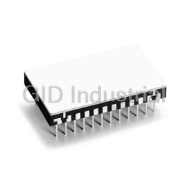
Single ADC SAR 12-bit Parallel 32-Pin CTDIP
5962-8850801XA
Part Number
5962-8850801XA
Price
Request Quote
Manufacturer
MURATA POWER SOLUTIONS
Lead Time
Request Quote
Category
Semiconductors » Adc
Specifications
Manufacturer
Murata Power Solutions
Manufacturers Part #
5962-8850801XA
Lead Time
16 Week Lead Time
Industry Aliases
5962-8850801XA
Factory Pack Quantity
1
Datasheet

Extracted Text
ADC-HX, ADC-HZ Series 12-Bit, 8 and 20μsec Analog-to-Digital Converters PRODUCT OVERVIEW The ADC-HX and ADC-HZ Series are self- Both models have identical operation except for contained, high-performance, 12-bit A/D convert- conversion speed. They can be short-cycled to give ers manufactured with thick and thin-fi lm hybrid faster conversions in lower-resolution applica- technology. They use the successive approximation tions. Use of the internal buffer amplifi er increases conversion technique to achieve a 12-bit conver- conversion time by 3 microseconds, the settling sion in 20 and 8 microseconds, respectively. Five time of the amplifi er. Output coding is comple- input voltage ranges are programmable by external mentary binary, complementary offset binary, or pin connection. An internal buffer amplifi er is also complementary two’s complement. Serial data is FEA FEATURES TURES provided for applications in which 50 megohm also brought out. The package is a 32-pin ceramic input impedance is required. TDIP. Models are available for use in commercial 12-bit resolution These converters utilize a fast 12-bit monolithic (0 to +70°C), industrial (–40 to +100°C), or military 8 or 20 microsecond conversion times DAC which includes a precision zener reference (–55 to +125°C) operating temperature ranges. 5 input voltage ranges source. The circuit also contains a fast mono- MIL-STD-883 and DESC Standard Military Drawing Internal high Z input buffer lithic comparator, a monolithic 12-bit successive models are also available. approximation register, a clock and a monolithic Short-cycle operation buffer amplifi er. Nonlinearity is specifi ed at INPUT/OUTPUT CONNECTIONS MIL-STD-883 models available Pin Function Pin Function ±1/2LSB maximum. 1 BIT 12 (LSB) 32 SERIAL DATA OUTPUT 2 BIT 11 31 –15V POWER 3 BIT 10 30 BUFFER INPUT 4 BIT 9 29 BUFFER OUTPUT 5 BIT 8 28 +15V POWER 6 BIT 7 27 GAIN ADJUST 7 BIT 6 26 ANALOG COMMON 8 BIT 5 25 20V INPUT RANGE 9 BIT 4 24 10V INPUT RANGE 10 BIT 3 23 BIPOLAR OFFSET 11 BIT 2 22 COMPARATOR INPUT 12 BIT 1 (MSB) 21 START CONVERT 13 BIT 1 (MSB) 20 E.O.C. (STATUS) 14 SHORT CYCLE 19 CLOCK OUT 15 DIGITAL COMMON 18 REFERENCE OUT +15V POWER –15V POWER REF. OUT +5V POWER 16 +5V POWER 17 CLOCK RATE 28 31 18 16 BUFFER BUFFER 30 + AMPLIFIER INPUT 6.3k� GAIN PRECISION 27 REF (+6.3V) ADJUST BUFFER 29 OUTPUT BIPOLAR 23 OFFSET DIGITAL 15 COMMON 12-BIT DAC COMPARATOR 22 INPUT COMPARATOR 5k� 10V SHORT 14 24 INPUT CYCLE SUCCESSIVE 5k� E.O.C. APPROXIMATION 20 STATUS REGISTER 20V 25 INPUT CLOCK ANALOG 26 COMMON 17 19 21 1 2 3 4 5 6 7 8 9 10 11 12 13 32 12 11 10 9 8 7 6 5 4 3 2 1 1 CLOCK CLOCK START SERIAL LSB. MSB MSB RATE OUT CONV. BIT NO. DATA OUT PARALLEL DATA OUT Figure 1. Functional Block Diagram DATEL, Inc. 11 Cabot Boulevard, MansŢ eld, MA 02048-1151 USA • Tel: (508) 339-3000 • www.datel.com • e-mail: help@datel.com ADC-HXHZ.C01 Page 1 of 7 ADC-HX, ADC-HZ Series 12-Bit, 8 and 20μsec Analog-to-Digital Converters ABSOLUTE MAXIMUM RATINGS POWER REQUIREMENTS Power Supply Voltages +15V ±0.5V at +20mA PARAMETERS LIMITS UNITS –15V ±0.5V at –25mA +15V Supply, Pin 28 +18 Volts +5V ±0.25V at +85mA –15V Supply, Pin 31 –18 Volts PHYSICAL/ENVIRONMENTAL +5V Supply, Pin 16 +7 Volts Digital Inputs, Pins 14, 21 ±5.5 Volts Operating Temp. Range, Case 0 to +70°C, –40 to +100°C, –55 to +125°C Analog Inputs, Pins 24, 25 ±25 Volts Storage Temperature Range –65 to +150°C Buffer Input, Pin 30 ±15 Volts Package Type 32-pin ceramic TDIP Lead Temperature (10 seconds) 300 °C Weight 0.5 ounces (14 grams) Thermal Impedance θ 6°C/W JC Functional SpeciŢ cations θ 30°C/W JA (Typical at +25°C and ±15V and +5V supplies unless otherwise noted) Footnotes: INPUTS ADC-HX12B ADC-HZ12B ➀ Adjustable to zero. Analog Input Ranges ➁ FSR is full scale range and is 10V for 0 to +10V or ±5V inputs and 20V for Unipolar 0 to +5V, 0 to +10V ±10V input, etc. Bipolar ±2.5V, ±5V, ±10V ➂ Without buffer amplifi er used. ADC-HZ may require external adjustment Input Impedance 2.5k (0 to +5V, ±2.5V) of clock rate. 5k (0 to +10V, ±5V) ➃ Short cycled operation. 10k (±10V) ➄ All digital outputs can drive 2 TTL loads. Input Impedance with Buffer 50 megohms Input Bias Current of Buffer 125nA typical, 250nA max. TECHNICAL NOTES Start Conversion +2V min. to +5.5V max. positive pulse with dur- 1. It is recommended that the ±15V power input pins both be bypassed to ground with a 0.01μF ceramic ation of 100ns min. Rise and fall times <30ns. capacitor in parallel with a 1μF electrolytic capacitor and the +5V power input pin be bypassed to ground with a 10μF electrolytic capacitor as shown in the connection diagrams. In addition, GAIN ADJUST (pin 27) Logic "1" to "0" transition resets converter and should be bypassed to ground with a 0.01μF ceramic capacitor. These precautions will assure noise free initiates next conversion. Loading: 2 TTL loads. operation of the converter. PERFORMANCE 2. DIGITAL COMMON (pin 15) and ANALOG COMMON (pin 26) are not connected together internally, and therefore must be connected as directly as possible externally. It is recommended that a ground plane be Resolution 12 bits run underneath the case between the two commons. Analog ground and ±15V power ground should be Nonlinearity ±1/2LSB max. run to pin 26 whereas digital ground and +5V ground should be run to pin 15. Differential Nonlinearity ±3/4LSB max. 3. External adjustment of zero or offset and gain are made by using trimming potentiometers connected as Accuracy Error ➀ shown in the connection diagrams. The potentiometer values can be between 10k and 100k Ohms and Gain (before adjustment) ±0.2% should be 100ppm/°C cermet types. The trimming pots should be located as close as possible to the con- Zero, Unipolar (before adj.) ±0.1% of FSR ➁ verter to avoid noise pickup. In some cases, for example 8-bit short-cycled operation, external adjustment may not be necessary. Offset, Bipolar (before adj.) ±0.2% of FSR ➁ Temperature CoefŢ cient 4. Short-cycled operation results in shorter conversion times when the conversion is truncated to less than 12 bits. This is done by connecting SHORT CYCLE (pin 14) to the output bit following the last bit desired. Gain ±20ppm/°C max. For example, for an 8-bit conversion, pin 14 is connected to the bit 9 output. Maximum conversion times Zero, Unipolar ±5ppm/°C of FSR max. ➁ are given for short-cycled conversions of 8 or 10 bits. In these two cases, the clock rate is accelerated by Offset, Bipolar ±10ppm/°C of FSR max. ➁ connecting the CLOCK RATE adjust (pin 17) to +5V (10 bits) or +15V (8 bits). The clock rate should not be Diff. Nonlinearity Tempco ±2ppm/°C of FSR max. ➁ arbitrarily speeded up to exceed the maximum conversion rate at a given resolution, as missing codes will No Missing Codes Over opererating temperature range result. Conversion Time ➂ 5. Note that output coding is complementary coding. For unipolar operation it is complementary binary, and 12 Bits 20μs max. 8μs max. for bipolar operation it is complementary offset binary or complementary two’s complement. In cases in which bipolar coding of offset binary or two’s complement is required, this can be achieved by inverting the 10 Bits ➃ 15μs max. 6μs max. analog input to the converter (using an op amp connected for gain of –1). The converter is then calibrated 8 Bits ➃ 10μs max. 4μs max. so that –FS analog input gives an output code of 0000 0000 0000, and +FS – 1LSB gives 1111 1111 1111. Buffer Settling Time (10V step) 3μs to ±0.01% 6. These converters can be operated with an external clock. To accomplish this, a negative pulse train is Power Supply Rejection ±0.004%/% supply max. applied to START CONVERT (pin 21). The rate of the external clock must be lower than the rate of the internal clock as adjusted (see Short Cycle Operation tables) for the converter resolution selected. The OUTPUTS ➄ pulse width of the external clock should be between 100 and 300 nanoseconds. Each N-bit conversion Parallel Output Data 12 parallel lines of data held until next cycle requires a pulse train of N + 1 clock pulses for completion, e.g., an 8-bit conversion requires 9 clock conversion command. pulses for completion. A continuous pulse train may be used for consecutive conversions, resulting in an V ("0") ≤ +0.4V N-bit conversion every N + 1 pulses, or the E.O.C. output may be used to gate a continuous pulse train for OUT single conversions. V ("1") ≥ +2.4V OUT 7. When the input buffer amplifi er is used, a delay equal to its settling time must be allowed between the input Unipolar Coding Complementary binary level change, such as a multiplexer channel change, and the negative-going edge of the START CONVERT Bipolar Coding Complementary offset binary pulse. If the buffer is not required, BUFFER INPUT (pin 30) should be tied to ANALOG COMMON (pin 26). This Complementary two’s complement prevents the unused amplifi er from introducing noise into the converter. For applications not using the buffer, Serial Output Data NRZ successive decision pulses out, MSB fi rst. the converter must be driven from a source with an extremely low output impedance. Compl. binary or compl. offset binary coding. End of Conversion (Status) Conversion status signal. Output is logic "1" during reset and conversion and logic "0" when conversion complete. Clock Output Train of positive going +5V 100ns pulses. 600kHz for ADC-HX and 1.5MHz for ADC-HZ (pin 17 grounded). Internal Reference +6.3V Reference Tempco ±20ppm/°C max. External Reference Current 2.5mA max. DATEL, Inc. 11 Cabot Boulevard, MansŢ eld, MA 02048-1151 USA • Tel: (508) 339-3000 • www.datel.com • e-mail: help@datel.com ADC-HXHZ.C01 Page 2 of 7 ADC-HX, ADC-HZ Series 12-Bit, 8 and 20μsec Analog-to-Digital Converters CODING TABLES UNIPOLAR OPERATION BIPOLAR OPERATION INPUT RANGE COMP. BINARY CODING INPUT VOLTAGE RANGE COMP. OFFSET BINARY COMP. TWO’S COMPLEMENT 0 TO +10V 0 TO +5V MSB LSB +10V +5V +2.5V MSB LSB MSB LSB +9.9976V +4.9988V 0000 0000 0000 +9.9951V +4.9976V + 2.4988V 0000 0000 0000 1000 0000 0000 +8.7500 +4.3750 0001 1111 1111 +7.5000 +3.7500 + 1.8750 0001 1111 1111 1001 1111 1111 + 7.5000 +3.7500 0011 1111 1111 +5.0000 +2.5000 + 1.2500 0011 1111 1111 1011 1111 1111 +5.0000 +2.5000 0111 1111 1111 0.0000 0.0000 0.0000 0111 1111 1111 1111 1111 1111 +2.5000 + 1.2500 1011 1111 1111 -5.0000 -2.5000 -1.2500 1011 1111 1111 0011 1111 1111 + 1.2500 +0.6250 1101 1111 1111 -7.5000 -3.7500 -1.8750 1101 1111 1111 0101 1111 1111 +0.0024 + 0.0012 1111 1111 1110 -9.9951 -4.9976 -2.4988 1111 1111 1110 0111 1111 1110 0.0000 0.0000 1111 1111 1111 -10.0000 -5.0000 -2.5000 1111 1111 1111 0111 1111 1111 SHORT CYCLE OPERATION Refer to Technical Note 4 for methods of reducing the ADC-HX or ADC-HZ conversion times. CONNECTIONS 8, 10 & 12-BIT CONVERSION TIMES �� �� ��� RESOLUTION 12 BITS 10 BITS 8 BITS ADC-HX Conversion Time 20μs 15μs 10μs ����� ���� �� ���� ADC-HZ Conversion Time 8μs 6μs 4μs �� 17 & 15 17 & 16 17 & 28 Connect These Pins Together ����� 14 & 16 14 & 2 14 & 4 ����� ����������� PIN 14 CONNECTION ��������������� RES. (BITS) PIN 14 TO RES. (BITS) PIN 14 TO 1 PIN 11 7 PIN 5 CLOCK RATE VS. VOLTAGE CLOCK RATE PIN 17 2 PIN 10 8 PIN 4 VOLTAGE ADC-HX ADC-HZ 3 PIN 9 9 PIN 3 600kHZ 1.5MHZ 4 PIN 8 10 PIN 2 0V 720kHZ 1.8MHz 5 PIN 7 11 PIN 1 +5V 6 PIN 6 12 PIN 16 880kHz 2.2MHz +15V DATEL, Inc. 11 Cabot Boulevard, MansŢ eld, MA 02048-1151 USA • Tel: (508) 339-3000 • www.datel.com • e-mail: help@datel.com ADC-HXHZ.C01 Page 3 of 7 ADC-HX, ADC-HZ Series 12-Bit, 8 and 20μsec Analog-to-Digital Converters START CONVERT IN +5V 16 17 + 15 18 +15V 10µF 14 19 13 20 ZERO 10k� 12 ADJUST 21 TO +5V COMMON 11 22 ANALOG INPUT 100k� 2.2M� 10 (–5 TO +5V) 23 ������ 9 24 �� 8 25 ������� 15V DATA 7 26 COMMON 0.01µF 2.8M� 10k� OUTPUTS 6 27 TO 5 28 100k� + GAIN 0.01 4 29 ADJUST µF 3 30 –15V 2 31 0.01 1 32 + µF 1µF 0.01µF CAPS ARE CERAMIC TYPES CAP Figure 2. Unipolar Operation, 0 to +10V START CONVERT IN +5V 16 17 + 15 18 +15V 10µF 14 19 13 20 OFFSET 10k� 12 ADJUST 21 TO +5V COMMON 11 22 ANALOG INPUT 100k� 2.2M� 10 (0 TO +10V) 23 ������ 9 �� 24 ������� 8 25 15V DATA 7 26 0.01µF 2.8M� COMMON 10k� OUTPUTS 6 27 TO 5 28 100k� + GAIN 0.01 4 29 ADJUST µF 3 30 2 31 –15V 0.01 1 32 + µF 1µF 0.01µF CAPS ARE CERAMIC TYPES CAP Figure 3. Bipolar Operation, –5 to +5V CONNECTIONS AND CALIBRATION INPUT CONNECTIONS WITHOUT BUFFER WITH BUFFER INPUT VOLTAGE RANGE INPUT PIN CONNECT THESE PINS TOGETHER INPUT PIN CONNECT THESE PINS TOGETHER 0 to +5V 24 22 & 25 23 & 26 30 22 & 25 23 & 26 29 & 24 0 to +10V 24 — 23 & 26 30 — 23 & 26 29 & 24 ±2.5V 24 22& 25 23 & 22 30 22 & 25 23 & 22 29 & 24 ±5V 24 — 23 & 22 30 — 23 & 22 29 & 24 ±10V 25 — 23 & 22 30 — 23 & 22 29 & 25 DATEL, Inc. 11 Cabot Boulevard, MansŢ eld, MA 02048-1151 USA • Tel: (508) 339-3000 • www.datel.com • e-mail: help@datel.com ADC-HXHZ.C01 Page 4 of 7 ADC-HX, ADC-HZ Series 12-Bit, 8 and 20μsec Analog-to-Digital Converters CALIBRATION PROCEDURE CALIBRATION TABLE UNIPOLAR RANGE ADJUST. INPUT VOLTAGE 1. Connect the converter for bipolar or unipolar operation. 0 to + 5V ZERO + 0.6 mV Use the input connection table for the desired input voltage range and GAIN + 4.9982V input impedance. Apply START CONVERT pulses of 100 nanoseconds ZERO + 1.2 mV 0 to + 10V minimum duration to pin 21. The spacing of the pulses should be no GAIN + 9.9963V less than the maximum conversion time. BIPOLAR RANGE 2. Zero and Offset Adjustments ± 2.5V OFFSET -2.4994V Apply a precision voltage reference source between the selected analog GAIN + 2.4982V input and ground. Adjust the output of the reference source to the OFFSET – 4.9988V ± 5V value shown in the Calibration Table for the unipolar zero adjustment GAIN + 4.9963V (zero + 1/2LSB) or the bipolar offset adjustment (–FS + 1/2LSB). Adjust OFFSET – 9.9976V ± 10V the trimming potentiometer so that the output code fl ickers equally GAIN + 9.9927V between 1111 1111 1111 and 1111 1111 1110. 3. Full Scale Adjustment Change the output of the precision voltage reference source to the value shown in the Calibration Table for the unipolar or bipolar gain adjustment (+FS – 1.5LSB). Adjust the gain trimming potentiometer so that the output code fl ickers equally between 0000 0000 0001 and 0000 0000 0000. TIMING DIAGRAM FOR ADC-HX, ADC-HZ OUTPUT: 101010101010 1 START 100ns min. CONVERT 0 60ns 1 E.O.C. PARALLEL DATA T1 (STATUS) NOW VALID 0 40ns 50ns 100ns CLOCK 1 5 8 9 1 2 3 4 6 7 10 11 12 13 OUT T2 0 40ns 1 SERIAL BIT 1 BIT 2 BIT 3 BIT 4 BIT 5 BIT 6 BIT 7 BIT 8 BIT 9 BIT 10 BIT 11 BIT 12 DATA OUT (LSB) (MSB) 0 40ns 1 BIT 1 (MSB) 0 1 BIT 2 0 1 BIT 3 0 1 BIT 12 (LSB) 0 TIMING DIAGRAM OPERATING PERIODS ADC-HX ADC-HZ T1 20μs 8μs T2 1.56μs 0.56μs DATEL, Inc. 11 Cabot Boulevard, MansŢ eld, MA 02048-1151 USA • Tel: (508) 339-3000 • www.datel.com • e-mail: help@datel.com ADC-HXHZ.C01 Page 5 of 7 ADC-HX, ADC-HZ Series 12-Bit, 8 and 20μsec Analog-to-Digital Converters MECHANICAL DIMENSIONS INCHES (mm) 1.72 MAX. (43.69) ���������������������(unless otherwise indicated): 2 place decimal (.XX) ±0.010 (±0.254) 32 17 3 place decimal (.XXX) ±0.005 (±0.127) ���������������Kovar alloy �������������50 microinches (minimum) gold plating 1.11 MAX. over 100 microinches (nominal) nickel plating (28.19) 1 16 0.100 TYP. 0.235 MAX. (2.540) (5.969) 1.500 (38.100) 0.200 MAX. (5.080) 0.010 ±0.002 (0.254) SEATING 0.190 MAX. 0.018 ±0.002 0.100 0.900 ±0.010 0.100 PLANE (4.826) (0.457) (2.540) (22.860) (2.540) 0.025 (0.635) 0.040 � (1.016) DATEL, Inc. 11 Cabot Boulevard, MansŢ eld, MA 02048-1151 USA • Tel: (508) 339-3000 • www.datel.com • e-mail: help@datel.com ADC-HXHZ.C01 Page 6 of 7 ADC-HX, ADC-HZ Series 12-Bit, 8 and 20μsec Analog-to-Digital Converters ORDERING GUIDE MODEL NUMBER TEMPERATURE RANGE SEAL ROHS ADC-HX12BGC 0 to +70°C Epoxy No ADC-HX12BGC-C 0 to +70°C Epoxy Yes ADC-HX12BMC 0 to +70°C Hermetic No ADC-HX12BMC-C 0 to +70°C Hermetic Yes ADC-HX12BME -40 to +100°C Hermetic No ADC-HX12BME-C -40 to +100°C Hermetic Yes ADC-HX12BME-QL -40 to +100°C Hermetic No ADC-HX12BME-QL-C -40 to +100°C Hermetic Yes ADC-HX12BMM -55 to +125°C Hermetic No ADC-HX12BMM-C -55 to +125°C Hermetic Yes ADC-HX12BMM-QL -55 to +125°C Hermetic No ADC-HX12BMM-QL-C -55 to +125°C Hermetic Yes ADC-HX/883 -55 to +125°C Hermetic No ADC-HZ12BGC 0 to +70°C Epoxy No ADC-HZ12BGC-C 0 to +70°C Epoxy Yes ADC-HZ12BMC 0 to +70°C Hermetic No ADC-HZ12BMC-C 0 to +70°C Hermetic Yes ADC-HZ12BME -40 to +100°C Hermetic No ADC-HZ12BME-C -40 to +100°C Hermetic Yes ADC-HZ12BME-QL -40 to +100°C Hermetic No ADC-HZ12BME-QL-C -40 to +100°C Hermetic Yes ADC-HZ12BMM -55 to +125°C Hermetic No ADC-HZ12BMM-C -55 to +125°C Hermetic Yes ADC-HZ12BMM-QL -55 to +125°C Hermetic No ADC-HZ12BMM-QL-C -55 to +125°C Hermetic Yes ADC-HZ/883 -55 to +125°C Hermetic No 5962-8850801XC -55 to +125°C Hermetic No 5962-8850802XC -55 to +125°C Hermetic No 5962-8850801XA -55 to +125°C Hermetic No 5962-8850802XA -55 to +125°C Hermetic No DATEL is a registered trademark of DATEL, Inc. DATEL, Inc. makes no representation that the use of its products in the circuits described herein, or the use of other technical information contained herein, will not infringe upon existing or future patent rights. The descriptions contained herein do not imply the granting of 11 Cabot Boulevard, MansŢ eld, MA 02048-1151 USA licenses to make, use, or sell equipment constructed in accordance therewith. Specifi cations are subject to change without notice. ITAR and ISO 9001/14001 REGISTERED © 2015 DATEL, Inc. www.datel.com • e-mail: help@datel.com ADC-HXHZ.C01 Page 7 of 7
Frequently asked questions
How does Electronics Finder differ from its competitors?

Is there a warranty for the 5962-8850801XA?
Which carrier will Electronics Finder use to ship my parts?
Can I buy parts from Electronics Finder if I am outside the USA?
Which payment methods does Electronics Finder accept?
Why buy from GID?

Quality
We are industry veterans who take pride in our work

Protection
Avoid the dangers of risky trading in the gray market

Access
Our network of suppliers is ready and at your disposal

Savings
Maintain legacy systems to prevent costly downtime

Speed
Time is of the essence, and we are respectful of yours
Related Products
Single ADC Pipelined 2Msps 12-bit Parallel 24-Pin CDDIP SMD ADS-117GC
Single ADC Pipelined 2Msps 12-bit Parallel 24-Pin CDDIP SMD ADS-117GM
Dual ADC Pipelined 5Msps 12-bit Parallel ADS-118/883UNREL
Single ADC 2-Step Flash 500ksps 14-bit Parallel 24-Pin CDDIP ADS-916MM
Single ADC 2-Step Flash 1Msps 14-bit Parallel 24-Pin CDDIP SMD ADS-927GM
Single ADC 2-Step Flash 2Msps 16-bit Parallel 40-Pin CTDIP ADS-932ME
Request a Quote

The quote request has been received
Close

Facing challenges or have inquiries? Feel free to contact us!
Call Us +1-469-283-2440
What they say about us
FANTASTIC RESOURCE
One of our top priorities is maintaining our business with precision, and we are constantly looking for affiliates that can help us achieve our goal. With the aid of GID Industrial, our obsolete product management has never been more efficient. They have been a great resource to our company, and have quickly become a go-to supplier on our list!
Bucher Emhart Glass
EXCELLENT SERVICE
With our strict fundamentals and high expectations, we were surprised when we came across GID Industrial and their competitive pricing. When we approached them with our issue, they were incredibly confident in being able to provide us with a seamless solution at the best price for us. GID Industrial quickly understood our needs and provided us with excellent service, as well as fully tested product to ensure what we received would be the right fit for our company.
Fuji
HARD TO FIND A BETTER PROVIDER
Our company provides services to aid in the manufacture of technological products, such as semiconductors and flat panel displays, and often searching for distributors of obsolete product we require can waste time and money. Finding GID Industrial proved to be a great asset to our company, with cost effective solutions and superior knowledge on all of their materials, it’d be hard to find a better provider of obsolete or hard to find products.
Applied Materials
CONSISTENTLY DELIVERS QUALITY SOLUTIONS
Over the years, the equipment used in our company becomes discontinued, but they’re still of great use to us and our customers. Once these products are no longer available through the manufacturer, finding a reliable, quick supplier is a necessity, and luckily for us, GID Industrial has provided the most trustworthy, quality solutions to our obsolete component needs.
Nidec Vamco
TERRIFIC RESOURCE
This company has been a terrific help to us (I work for Trican Well Service) in sourcing the Micron Ram Memory we needed for our Siemens computers. Great service! And great pricing! I know when the product is shipping and when it will arrive, all the way through the ordering process.
Trican Well Service
GO TO SOURCE
When I can't find an obsolete part, I first call GID and they'll come up with my parts every time. Great customer service and follow up as well. Scott emails me from time to time to touch base and see if we're having trouble finding something.....which is often with our 25 yr old equipment.
ConAgra Foods