

 Manufacturers
CITIZEN SYSTEMS AMERICA BD2-2880U
Description
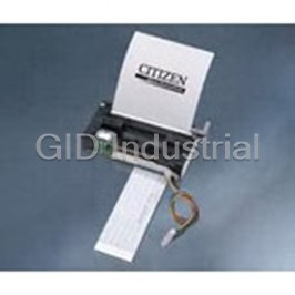
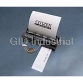
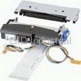
Control Boards Is Designed To Be Used To Control Our Thermal Printer
BD2-2880U
Part Number
BD2-2880U
Price
Request Quote
Manufacturer
CITIZEN SYSTEMS AMERICA
Lead Time
Request Quote
Category
Tools and Supplies » Development Kits and Tools
Specifications
Manufacturer
Citizen Systems America
Manufacturers Part #
BD2-2880U
Sub-Category
Development Kits and Tools
Series
CB
Factory Pack Quantity
1
Datasheet

Extracted Text
User’s Manual
CONTROL BOARD FOR MLT-288/MLT-289
MODEL
BD2-2880/2890
Rev. 1.10 Newly Issued on June 23rd, 2003
REVISION
Rev. No. Date Content
0.00 2000.06.26 Newly authored as a tentative edition for CS products reference.
1.00 2002.08.09 Cover, Page 1, 2, 3, 7, 9 is changed.
1.10 2003.06.23 Chapters 11 (Print Control Functions) and 12 (Character Code Table)
are deleted.
i
CONTENTS
1. OUTLINE ........................................................................................................................ 1
1.1 Features ............................................................................................................................................................. 1
1.2 Precaution .......................................................................................................................................................... 1
2. BASIC SPECIFICATIONS ........................................................................................... 2
2.1 Model Classification.......................................................................................................................................... 2
2.2 Basic Specifications........................................................................................................................................... 3
3. CONNECTING CONNECTORS.................................................................................. 4
3.1 CN1 Connector for Printer Mechanism (For Print Head) ................................................................................. 4
3.2 CN2 Connector for Print Mechanism (For Motor & Sensor)............................................................................ 4
3.3 CN3 Connector for Interface ............................................................................................................................. 5
3.4 CN4 Connector for Paper Cutter ....................................................................................................................... 6
4. DIP SWITCH SETTING ............................................................................................... 7
5. POWER SUPPLY ........................................................................................................... 9
5.1 Specifications .................................................................................................................................................... 9
5.2 Precautions ........................................................................................................................................................ 9
6. PARALLEL INTERFACE ........................................................................................... 10
6.1 Specifications .................................................................................................................................................. 10
6.2 Explanation of Input/Output Signals ............................................................................................................... 10
6.3 Electrical Characteristics ................................................................................................................................. 10
6.4 Timing Chart.................................................................................................................................................... 11
6.5 Data Receiving Control ................................................................................................................................... 12
6.6 Buffering.......................................................................................................................................................... 12
7. SERIAL INTERFACE ................................................................................................. 13
7.1 Specifications .................................................................................................................................................. 13
7.2 Explanation of Input/Output Signals ............................................................................................................... 14
7.3 Error Detection ................................................................................................................................................ 14
7.4 Data Receiving Control ................................................................................................................................... 14
7.5 Buffering.......................................................................................................................................................... 15
7.6 Electrical Characteristics ................................................................................................................................. 15
ii
8. ERROR HANDLING ................................................................................................... 16
8.1 Peripheral Circuit Errors ................................................................................................................................. 16
8.2 Operation Errors .............................................................................................................................................. 16
8.3 Errors Indication .............................................................................................................................................. 18
9. PRINTER MECHANISM CONTROL SYSTEM ..................................................... 19
9.1 Thermal Head Control System (Division Driving System)............................................................................. 19
9.1.1 Fixed Division Number System ................................................................................................................. 19
9.1.2 Variable Division Number System ............................................................................................................. 19
9.2 Motor Drive ..................................................................................................................................................... 20
9.2.1 Motor Drive Features ................................................................................................................................. 20
9.2.2 Maximum Motor Drive Speeds at Major Voltage ...................................................................................... 20
10. MAINTENANCE AND SERVICE............................................................................ 21
APPENDIX 1. BLOCK DIAGRAM ............................................................................... 22
APPENDIX 2. OUTER DIMENSION ............................................................................ 23
iii
BD2-2880/2890 User’s Manual
1. OUTLINE
This control boards is designed to be used to control our thermal printer, “MLT-288/289” series
through the computer etc.
As being provided with many abundant functions, it can be used widely in various applications.
Before you start using it, read this manual thoroughly and understand the content.
1.1 Features
(1) Ultra compact
(2) Both interface of Serial and Parallel can be selected by dip switch.
(3) Input buffer incorporated.
(4) Bar code printing is available (dedicated command).
(5) Auto paper cutter control incorporated.
(6) User-defined character registration function (94 characters)
(7) Low cost
1.2 Precaution
(1) Make sure to turn OFF the power supply in case of connecting/disconnecting the connectors.
(2) Absolutely do not make a short circuit between the terminals of connectors.
(3) Use power supply, LED, interface etc. following their specifications.
(4) Use the recommended paper shown below.
• Thermal Paper TF5KS-E2D (Nippon paper)
KF50-HDA (Shin-Oji paper)
F220VP, HP220A (Mitsubishi paper)
1
BD2-2880/2890 User’s Manual
2. BASIC SPECIFICATIONS
2.1 Model Classification
Models are identified by the following coding scheme:
BD2 - 2880 U C
Auto Cutter Drive
C : With auto cutter function
None : Without auto cutter function
Character Set
U : Internatiomal model
Model Name of applied printer mechanism
2880 : For MLT-288
2890 : For MLT-289
Model Name
2
BD2-2880/2890 User’s Manual
2.2 Basic Specifications
Items Contents
Printing system Thermosensitive dot-matrix printing
Print width 48 mm
Print Speed 420 dot line/sec
Font A : 32 columns
Number of columns
Font B : 42 columns
Font A : 1.25 mm × 3.00 mm
Character dimensions
Font B : 0.88 mm × 3.00 mm
Character types Alphanumeric, international characters
Bar code type UPC-A/E, JAN (EAN) 13/8 columns, ITFCODE 39, CODE128, CODABAR
Line pitch 4.23 mm (Can be changed by command)
Interface Parallel (Conforms to Centronics) or Serial (Conforms to RS-232C) (Selectable by dip switch)
Input buffer 2 K bytes
VCC: 5V ± 5 % Approx. 130 mA (Self printing)
VP : 4.2V ~ 8.5V Approx. 1.5A (Ave) Approx. 4A (Peak) When 7.2V
Supply voltage
Ordinal voltage is to be 7.2V (Max)
8.5V is a voltage, which is right after charging.
Weight Approx. 40 g
Outer Dimension 75 mm (W) × 80 mm (D) (For height of component parts, see outer drawing.)
Operating Environment 5 ~ 40˚C , 35 ~ 85% RH (with no dew condensation)
Storage Environment -20 ~ 60˚C , 10 ~ 90% RH (with no dew condensation)
3
BD2-2880/2890 User’s Manual
3. CONNECTING CONNECTORS
3.1 CN1 Connector for Printer Mechanism (For Print Head)
Pin No. Signal Name I/O Function
1 VH –
Power for print head
2 VH –
Power for print head
3 SI Output
Head data output signal
4 GND –
GND
5 TM Input
Thermistor
6 STRB 1 Output
Strobe 1
7 STRB 2 Output
Strobe 2
8 Vdd –
Thermal head logics power (+5V)
9 LATCH Output
Latch signal
10 GND –
GND
11 STRB 6 Output
Strobe 6
12 CP Output
Clock pulse
13 GND –
GND
14 STRB 5 Output
Strobe 5
15 STRB 3 Output
Strobe 3
16 GND –
GND
17 GND –
GND
18 STRB 4 Outpu
Strobe 4
19 GND –
GND
20 GND –
GND
21 GND –
GND
22 VH –
Power for print head
23 VH –
Power for print head
24 VH –
Power for print head
Applicable Connector : 52806-2410 (Molex)
3.2 CN2 Connector for Print Mechanism (For Motor & Sensor)
Pin No. Signal Name I/O Function
1 MOTOR B Output Operation signal for motor B
2 MOTOR A Output Operation signal for motor A
3 MOTOR B Output Operation signal for motor B
4 MOTOR A Output Operation signal for motor A
5 PE C Input Photo-transistor collector (Paper sensor)
6 GND – Photinterruptor emitter + cathode
7 PE A – Photo-LED anode (Paper sensor)
8 H-UP Input Head-up signal
9 GND – Head-up sensor GND
Applicable Connector : 53047-0910 (Molex)
4
BD2-2880/2890 User’s Manual
3.3 CN3 Connector for Interface
Pin No. Signal Name I/O Function
1 Vcc ––
Power supply for circuit (5V)
2 Vcc ––
Power supply for circuit (5V)
3 GND ––
GND
4 GND ––
GND
5 Vp ––
Power supply for operation
6 Vp ––
Power supply for operation
7 Vp ––
Power supply for operation
8 Vp ––
Power supply for operation
9 Vp ––
Power supply for operation
10 Vp ––
Power supply for operation
11 P-GND ––
GND for operation
12 P-GND ––
GND for operation
13 P-GND ––
GND for operation
14 P-GND ––
GND for operation
15 P-GND ––
GND for operation
16 P-GND ––
GND for operation
17 LF-SW Input
LF Switch input
18 ERROR Output
ERROR LED output (Can be connected directly)
19 PEout Output
PE LED output (Can be connected directly)
20 DTR Output
Serial Interface DTR
21 TXD Output
Serial Interface TXD
22 RXD Input
Serial Interface RXD
23 DSR Input
Serial Interface DSR
24 DATA0 Output
Parallel Interface DATA0
25 DATA1 Output
Parallel Interface DATA1
26 DATA2 Output
Parallel Interface DATA2
27 DATA3 Output
Parallel Interface DATA3
28 DATA4 Output
Parallel Interface DATA4
29 DATA5 Output
Parallel Interface DATA5
30 DATA6 Output
Parallel Interface DATA6
31 DATA7 Output
Parallel Interface DATA7
32 STB Output
Parallel Interface STB
33 BUSY Output
Parallel Interface BUSY
34 FAULT Output
Parallel Interface FAULT
35 SELECT Output
Parallel Interface SELECT
36 PE Output
Parallel Interface PE
37 NC Output
Parallel Interface ACK
38 NC ––
No Connection
39 SELECTIN ––
No Connection
40 RESET Input
Parallel Interface RESET
Applicable Connector : 53313 - 4015 (Molex)
5
BD2-2880/2890 User’s Manual
CAUTION:
1. For LED of ERROR and PE, there is a resister of 330Ω on the circuit side to make current
value 10 mA.
Please use LED which its voltage is approx. 2V. LED over 10 mA may break a control board.
2. Control circuit requires power supply only for one pin of each VCC and GND.
However, Operation voltage is to be supplied to all of pin for safety use.
3. Serial interface equips a driver and receiver of RS-232C, make sure to use it at RS-232C
level.
4. RESET terminal is pulled up by 3.3KΩ. Make sure to make this terminal NC, when this
terminal is not used.
5. LF-SW input circuit is as below.
VCC
CN
47k
CPU
1k
1000pF
3.4 CN4 Connector for Paper Cutter
Pin No. Signal Name I/O Function
1 M+ Output Cutter motor operational signal M +
2 M– Output Cutter motor operational signal M –
3 GND –– GND
4 SW Input Cutter switch input signal
Using Connector : 5267- 04A-X (Molex)
Note: Use the specified Paper Cutter (Model Name : ACS-220-5V)
6
BD2-2880/2890 User’s Manual
4. DIP SWITCH SETTING
(1) DIP SWITCH
Pin No. Function ON OFF Factory Setting
DS1-1 Auto Cutter Enable Disable OFF
1-2 CR Selection LF Enable LF Disable ON
1-3 Print Density Combination with J-6 (See next page (5)) OFF
1-4 DTR/XON-XOFF XON-XOFF DTR/DSR OFF
1-5 Baud Rate OFF
1-6 OFF
"
See below (3)
1-7 OFF
"
1-8 OFF
"
(2) JUMPER
Pin No. Function Short Open Factory Setting
J1 International Character set
Short circuit
J2
See next page (4) Short circuit
"
J3
Short circuit
"
J4 Paper Auto Loading Enable
Disable Short circuit
J5 Print Drive System Variable division
Fixed division Short circuit
J6 Print Density
Combination with DS1-3 Short circuit
(Supplementary)
See next page (5)
J7 Not Used
– Short circuit
J8 Mechanism MLT-288 MLT-289 *1
Short circuit
*1 : BD2-2890 is set to open circuit.
(3) INTERFACE & BAUD RATE
DS1-8 DS1-7 DS1-6 DS1-5 Input Method Parity Baud Rate
OFF OFF OFF OFF Parallel Input –
–
OFF OFF OFF ON Serial Input None
1200 bps
OFF OFF ON OFF
2400 bps
" "
OFF OFF ON ON
4800 bps
" "
OFF ON OFF OFF
9600 bps
" "
OFF ON OFF ON
19200 bps
" "
OFF ON ON OFF Odd
1200 bps
"
OFF ON ON ON
2400 bps
" "
ON OFF OFF OFF
4800 bps
" "
ON OFF OFF ON
9600 bps
" "
ON OFF ON OFF
19200 bps
" "
ON OFF ON ON Even
1200 bps
"
ON ON OFF OFF
2400 bps
" "
ON ON OFF ON
4800 bps
" "
ON ON ON OFF
9600 bps
" "
ON ON ON ON
19200 bps
" "
7
BD2-2880/2890 User’s Manual
(4) INTERNATIONAL CHARACTER SET
J-3 J-2 J-1 InternationalCharacter
Open Open Open Japan (JIS)
Open Open Short Japan (Shift-JIS)
Open Short Open Sweden
Open Short Short Denmark 1
Short Open Open U.K.
Short Open Short Germany
Short Short Open France
Short Short Short U.S.A
(5) PRINT DENSITY
DS1-3 J-6 Print Density Level Print Density Rate
OFF Open Light 0 80%
OFF Short Standard 1 100%
ON Open Slightly Dark 2 120%
ON Short Dark 3 150%
Note:
1. Input Buffer is 2k byte. (Fixed)
2. Serial data length is 8 bits. (Fixed)
If print tone is set at 2 or above, printing rate tends to be lowered.
8
BD2-2880/2890 User’s Manual
5. POWER SUPPLY
5.1 Specifications
VCC : 5V ±5% Approx. 130 mA
VP : 4.2V ~ 8.5V Approx. 1.5A (Peak : Approx. 4A) when 7.2V
Ordinal Voltage is to be 7.2V (Max). 8.5V is a voltage that is right after charging.
8.5V cannot be used for ordinal voltage.
5.2 Precautions
(1) Design the product to supply power to Vcc before VP when power is supplied to this control
board.
(2) Design the product to turn off the power for Vcc after VP when power is turned off.
(3) Make sure to turn off the power in case of connecting/disconnecting connectors.
(4) Make sure to use Vcc and VP following their specifications.
(5) Make sure to use this control board connecting all of terminals between VP and P-GND.
9
BD2-2880/2890 User’s Manual
6. PARALLEL INTERFACE
6.1 Specifications
Data input method : 8 bit parallel signal (DATA0~7)
Control signals : ACK, BUSY, STB, FAULT, PE, RESET
6.2 Explanation of Input/Output Signals
DATA0~7 : 8 bit parallel signal (Positive logic)
STB : Strobe signal to read 8 bit data (Negative logic)
RESET : Signal to reset control board (Negative logic)
ACK : 8 bit data request signal. Pulse signal output at the end of the BUSY
signal (Negative logic)
BUSY : Signal to indicate BUSY state of the printer. Input new data for “LOW”
(Positive logic)
FAULT : Signal which is made “LOW” when printer is in alarm state.
(Negative logic)
In this case all the control logics within the printer stop functioning.
PE : Signal which is output when paper runs out. (Positive logic)
6.3 Electrical Characteristics
(1) Input Signal Level
“HIGH” level : 0.7 Vcc MIN
“LOW” level : 0.3 Vcc MAX
(2) Output Signal Level
“HIGH” level : Vcc - 0.1V MIN
“LOW” level : 0.1V MAX
10
BD2-2880/2890 User’s Manual
(3) I/O Conditions
STB, RESET input signals are pulled up by 3.3K .
Other input signals are pulled up by 50K .
[Host side]
[Printer side]
VCC
TWIST PAIR WIRE
All the output signals are pulled up by 50K
[Host side]
[Printer side]
VCC
TWIST PAIR WIRE
6.4 Timing Chart
(1) Data Input and Printing Timing
Power Supply
DATA
T2
STB
T1 T3
T6
BUSY T4
BUSY
ACK
T5
T1, T2, T3 : 0.5 µs (MIN)
T4 : 270 ns (MAX)
T5 : 2.3 µs (TYP)
T6 : 500 ms (MIN) *On supplying power
11
BD2-2880/2890 User’s Manual
6.5 Data Receiving Control
When BUSY signal is “LOW”, data from the host can be received. When it being “HIGH”, data
cannot be received.
6.6 Buffering
This control board incorporates 2K byte buffer.
Therefore, big data can be buffered in input buffer, and the host side can be released immediately.
12
BD2-2880/2890 User’s Manual
7. SERIAL INTERFACE
7.1 Specifications
(1) Data transfer system: Asynchronous
(2) Baud rates
1200, 2400, 4800, 9600, 19200 bps (Selectable by user)
(3) Configuration of one word
Start bit : 1 bit
Data bit : 8 bits Fixed
Parity bit : Odd/Even or No parity (Selectable by user)
Stop bit : 1 bit or more
(4) Signal polarity
RS-232C
• Mark = logic “ 1” (–3V ~ –12V)
• Space = logic “ 0” (+3V ~ +12V)
(5) Receiving data (RD signal)
RS-232C
• Mark = 1
• Space = 0
(6) Receiving control (DTR signal)
RS-232C
• Mark : Data transfer is not available
• Space : Data transfer is available
(7) Transmission control (TD signal)
DC1 code (11H) X-ON : Data reception is available
DC3 code (13H) X-OFF : Data reception is not available
13
BD2-2880/2890 User’s Manual
7.2 Explanation of Input/Output Signals
(1) RXD
Serial receiving data signal. On occurrence of framing error, overrun error, or parity error, the
data is printed as “?”.
(2) DTR
When this signal is READY, write data or a command. When they are written in BUSY, overrun
error is occurred and data is ignored. Data can be written into the input buffer even when the
printer is busy printing. A BUSY also occurs when the printer is powered on, in test print, in
Online mode, or being reset.
(3) TXD
If data remaining in the printer's input buffer is 256 bytes or less, the printer transfers a DC3
(13H: Data Receive Not Ready) signal to the host. If data in the input buffer exceeds 256 bytes,
the printer transfers a DC1 (11H: Data Receive Ready) signal to the host.
(4) GND
Common GND on the circuit.
7.3 Error Detection
Parity, framing, and overrun are detected. On detection of any error, the data are stored in the
buffer as “?”.
(1) Framing Error
With “space” state having been detected on detection of a stop bit, error takes place.
The data are stored in the buffer as “?”.
(2) Parity Error
With an error having been detected under specifying parity check, the data is stored in the buffer
as “?”.
(3) Overrun Error
On detection of an overrun error, the data are stored in the buffer as “?”.
7.4 Data Receiving Control
When DTR/DSR control having been selected, with BUSY signal at “LOW”, data from the host
side are received. With the signal at “HIGH”, they can not be received.
When DTR/DSR control not having been selected, after X-ON transmission, data is received
from the host side. No transmission of data can take place after X-OFF is transmitted.
14
BD2-2880/2890 User’s Manual
7.5 Buffering
Data transfer to the input buffer include DTR signals and TD signals as the control signals
concerned.
(1) DTR signals (See the page 7.2 (2))
(2) TXD signals (See the page 7.2 (3))
7.6 Electrical Characteristics
(1) RS-232C Circuit
Input (RXD, DSR)
Frequently asked questions
How does Electronics Finder differ from its competitors?

Is there a warranty for the BD2-2880U?
Which carrier will Electronics Finder use to ship my parts?
Can I buy parts from Electronics Finder if I am outside the USA?
Which payment methods does Electronics Finder accept?
Why buy from GID?

Quality
We are industry veterans who take pride in our work

Protection
Avoid the dangers of risky trading in the gray market

Access
Our network of suppliers is ready and at your disposal

Savings
Maintain legacy systems to prevent costly downtime

Speed
Time is of the essence, and we are respectful of yours
Related Products
Control Boards Is Designed To Be Used To Control Our Thermal Printer BD2-3880UC
Line Thermal Printer Mechanisms Board BD2-4281U
Request a Quote

The quote request has been received
Close

Facing challenges or have inquiries? Feel free to contact us!
Call Us +1-469-283-2440
What they say about us
FANTASTIC RESOURCE
One of our top priorities is maintaining our business with precision, and we are constantly looking for affiliates that can help us achieve our goal. With the aid of GID Industrial, our obsolete product management has never been more efficient. They have been a great resource to our company, and have quickly become a go-to supplier on our list!
Bucher Emhart Glass
EXCELLENT SERVICE
With our strict fundamentals and high expectations, we were surprised when we came across GID Industrial and their competitive pricing. When we approached them with our issue, they were incredibly confident in being able to provide us with a seamless solution at the best price for us. GID Industrial quickly understood our needs and provided us with excellent service, as well as fully tested product to ensure what we received would be the right fit for our company.
Fuji
HARD TO FIND A BETTER PROVIDER
Our company provides services to aid in the manufacture of technological products, such as semiconductors and flat panel displays, and often searching for distributors of obsolete product we require can waste time and money. Finding GID Industrial proved to be a great asset to our company, with cost effective solutions and superior knowledge on all of their materials, it’d be hard to find a better provider of obsolete or hard to find products.
Applied Materials
CONSISTENTLY DELIVERS QUALITY SOLUTIONS
Over the years, the equipment used in our company becomes discontinued, but they’re still of great use to us and our customers. Once these products are no longer available through the manufacturer, finding a reliable, quick supplier is a necessity, and luckily for us, GID Industrial has provided the most trustworthy, quality solutions to our obsolete component needs.
Nidec Vamco
TERRIFIC RESOURCE
This company has been a terrific help to us (I work for Trican Well Service) in sourcing the Micron Ram Memory we needed for our Siemens computers. Great service! And great pricing! I know when the product is shipping and when it will arrive, all the way through the ordering process.
Trican Well Service
GO TO SOURCE
When I can't find an obsolete part, I first call GID and they'll come up with my parts every time. Great customer service and follow up as well. Scott emails me from time to time to touch base and see if we're having trouble finding something.....which is often with our 25 yr old equipment.
ConAgra Foods