

 Manufacturers
MURATA POWER SOLUTIONS ADS-CCD1202MM-QL
Description
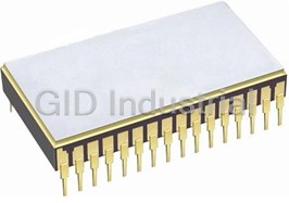
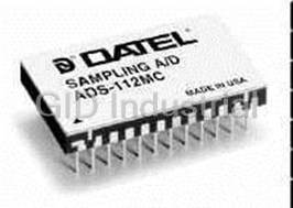
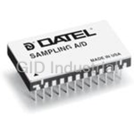
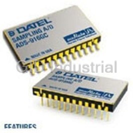
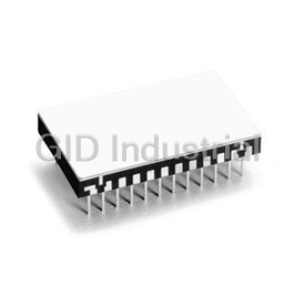
Single ADC Pipelined 2Msps 12-bit Parallel 24-Pin CDDIP
ADS-CCD1202MM-QL
Part Number
ADS-CCD1202MM-QL
Price
Request Quote
Manufacturer
MURATA POWER SOLUTIONS
Lead Time
Request Quote
Category
Semiconductors » Adc
Specifications
Manufacturer
Murata Power Solutions
Manufacturers Part #
ADS-CCD1202MM-QL
Lead Time
16 Week Lead Time
Factory Pack Quantity
1
Datasheet

Extracted Text
ADS-CCD1202 12-Bit, 2MHz, Sampling A/D’s for CCD Imaging Applications PRODUCT OVERVIEW The functionally complete, easy-to-use ADS- ±12V) and +5V supplies and typically consumes CCD1202 is a 12-bit, 2MHz Sampling A/D Con- 1.75 (1.45) Watts. The device is 100% production verter whose performance and production testing tested for all critical performance parameters and have been optimized for use in CCD applications. is fully specifi ed over both the 0 to +70°C and –55 This device delivers the lowest noise (600μVrms) to +125°C operating temperature ranges. and the best differential linearity error (±0.45LSB For those applications using correlated double maximum) of any commercially available 12-bit sampling, the ADS-CCD1202 can be supplied A/D in its speed class. It can respond to full scale without its internal sample-hold amplifi er and input steps (from empty to full well) with less than achieve conversion rates up to 2.5MHz. DATEL a single count of error, and its input is immune to will also entertain discussions about including the overvoltages that may occur due to blooming. CDS circuit internal to the ADS-CCD1202. Please Packaged in an industry-standard, 24-pin, contact us for more details. FEATURES ceramic DDIP, the ADS-CCD1202 requires ±15V (or Unipolar input range (0 to +10V) 2MHz sampling rate INPUT/OUTPUT CONNECTIONS PIN FUNCTION PIN FUNCTION 4096-to-1 dynamic range (72.2dB) 1 BIT 12 (LSB) 24 –12V/–15V SUPPLY 2 BIT 11 23 GROUND Low noise, 600μVrms (1/4 of an LSB) 3 BIT 10 22 +12V/+15V SUPPLY Outstanding differential nonlinearity error 4 BIT 9 21 +10V REFERENCE OUT (±0.45 LSB max.) 5 BIT 8 20 ANALOG INPUT 6 BIT7 19 GROUND Small, 24-pin ceramic DDIP 7 BIT 6 18 NO CONNECT 8 BIT 5 17 NO CONNECT Low power, 1.75 Watts 9 BIT 4 16 START CONVERT Operates from ±12V or ±15V supplies 10 BIT 3 15 EOC 11 BIT 2 14 GROUND Edge-triggered, no pipeline delay 12 BIT 1 (MSB) 13 +5V SUPPLY Low cost BLOCK DIAGRAM – ANALOG INPUT 20 S/H DAC + S2 12 BIT 1 (MSB) S1 11 BIT 2 10 BIT 3 +10V REFERENCE 21 REF 9 BIT 4 8 BIT 5 DIGITAL 7 BIT 6 REGISTER CORRECTION 6 BIT 7 LOGIC 5 BIT 8 FLASH 4 BIT 9 ADC 3 BIT 10 2 BIT 11 BUFFER REGISTER 1 BIT 12 (LSB) START CONVERT 16 TIMING AND CONTROL LOGIC EOC 15 13 17, 18 22 14, 19, 23 24 +5V SUPPLY NO CONNECT +12V/+15V SUPPLY GROUND –12V/–15V SUPPLY Figure 1. ADS-CCD1202 Functional Block Diagram DATEL, Inc. 11 Cabot Boulevard, MansŢ eld, MA 02048-1151 USA • Tel: (508) 339-3000 • www.datel.com • e-mail: help@datel.com 11 Sep 2015 MDA_ADS-CCD1202.B02 Page 1 of 9 ADS-CCD1202 12-Bit, 2MHz, Sampling A/D’s for CCD Imaging Applications ABSOLUTE MAXIMUM RATINGS PHYSICAL/ENVIRONMENTAL PARAMETERS LIMITS UNITS PARAMETERS MIN. TYP. MAX. UNITS +12V/+15V Supply (Pin 22) 0 to +16 Volts Operating Temp. Range, Case –12V/–15V Supply (Pin 24) 0 to –16 Volts ADS-CCD1202MC 0 — +70 °C +5V Supply (Pin 13) 0 to +6 Volts ADS-CCD1202MM –55 — +125 °C Digital Input (Pin 16) –0.3 to +VDD +0.3 Volts Thermal Impedance Analog Input (Pin 20) –5 to +14 Volts θjc — 5 — °C/Watt Lead Temp. (10 seconds) +300 °C θca — 24 — °C/Watt Storage Temperature Range –65 — +150 °C Package Type 24-pin, metal-sealed ceramic DDIP Weight 0.42 ounces (12 grams) FUNCTIONAL SPECIFICATIONS (TA = +25°C, ±Vcc = ±15V (or ±12V), +VDD = +5V, 2MHz sampling rate, and a minimum 1 minute warmup ➀ unless otherwise specifi ed.) +25°C 0 TO +70°C –55 TO +125°C ANALOG INPUT MIN. TYP. MAX. MIN. TYP. MAX. MIN. TYP. MAX. UNITS Input Voltage Range d — 0 to +10 — — 0 to +10 — — 0 to +10 — Volts Input Resistance 0.99 1 1.01 0.99 1 1.01 0.99 1 1.01 kΩ Input Capacitance — 7 15 — 7 15 — 7 15 pF DIGITAL INPUT Logic Levels Logic "1" +2.0 — — +2.0 — — +2.0 — — Volts Logic "0" — — +0.8 — — +0.8 — — +0.8 Volts Logic Loading "1" — — +20 — — +20 — — +20 μA Logic Loading "0" — — –20 — — –20 — — –20 μA Start Convert Positive Pulse Width ➂ — 200 — — 200 — — 200 — ns STATIC PERFORMANCE Resolution — 12 — — 12 — — 12 — Bits Integral Nonlinearity (fi n = 10kHz) — ±0.5 — — ±0.5 — — ±1 — LSB Differential Nonlinearity (fi n = 10kHz) — +0.25 ±0.45 — ±0.25 ±0.45 — ±0.35 ±0.75 LSB Full Scale Absolute Accuracy — +0.1 ±0.3 — ±0.2 ±0.5 — ±0.3 ±0.8 %FSR Offset Error (Tech Note 2) — ±0.15 ±0.3 — ±0.2 ±0.5 — ±0.5 ±1.2 %FSR Gain Error (Tech Note 2) — ±0.1 ±0.4 — ±0.4 ±0.8 — ±0.5 ±1.4 % No Missing Codes (fi n = 10kHz) 12 — — 12 — — 12 — — Bits DYNAMIC PERFORMANCE Peak Harmonics (–0.5dB) dc to 500kHz — –80 –75 — –80 –75 — –76 –72 dB 500kHz to 1MHz — –77 –71 — –77 –71 — –73 –66 dB Total Harmonic Distortion (–0.5dB) dc to 500kHz — –76 –73 — –76 –73 — –74 –70 dB 500kHz to 1MHz — –75 –70 — –75 –70 — –71 –65 dB Signal-to-Noise Ratio (w/o distortion, –0.5dB) dc to 500kHz 71 72 — 71 72 — 71 72 — dB 500kHz to 1MHz 71 72 — 71 72 — 70 72 — dB Signal-to-Noise Ratio f (& distortion, –0.5dB) dc to 500kHz 70 71 — 70 71 — 68 70 — dB 500kHz to 1MHz 68 71 — 68 71 — 65 69 — dB Two-Tone Intermodulation Distortion (fi n = 200kHz, 500kHz, fs = 2MHz, –0.5dB) — –83 — — –82 — — –81 — dB Noise — 600 — — 600 — — 600 — μVrms Input Bandwidth (–3dB) Small Signal (–20dB input) — 9 — — 9 — — 9 — MHz Large Signal(–0.5dB input) — 8 — — 8 — — 8 — MHz Feedthrough Rejection (fi n = 1MHz) — 82 — — 82 — — 82 — dB Slew Rate — ±200 — — ±200 — — ±200 — V/μs Aperture Delay Time — ±20 — — ±20 — — ±20 — ns Aperture Uncertainty — 5 — — 5 — — 5 — ps rms S/H Acquisition Time (to ±0.01%FSR, 10V step) 150 190 230 150 190 230 150 190 230 ns Overvoltage Recovery Time ➄ — 400 500 — 400 500 — 400 500 ns A/D Conversion Rate 2 — — 2 — — 2 — — MHz ANALOG OUTPUT Internal Reference Voltage +9.95 +10.0 +10.05 +9.95 +10.0 +10.05 +9.95 +10.0 +10.05 Volts Drift — ±5 — — ±5 — — ±5 — ppm/ºC External Current — — 1.5 — — 1.5 — — 1.5 mA DATEL, Inc. 11 Cabot Boulevard, MansŢ eld, MA 02048-1151 USA • Tel: (508) 339-3000 • www.datel.com • e-mail: help@datel.com 11 Sep 2015 MDA_ADS-CCD1202.B02 Page 2 of 9 ADS-CCD1202 12-Bit, 2MHz, Sampling A/D’s for CCD Imaging Applications +25°C 0 TO +70°C –55 TO +125°C DIGITAL OUTPUTS MIN. TYP. MAX. MIN. TYP. MAX. MIN. TYP. MAX. UNITS Logic Levels Logic "1" +2.4 — — +2.4 — — +2.4 — — Volts Logic "0" — — +0.4 — — +0.4 — — +0.4 Volts Logic Loading "1" — — –4 — — –4 — — –4 mA Logic Loading "0" — — +4 — — +4 — — +4 mA Delay, Falling Edge of EOC to Output Data Valid — — 35 — — 35 — — 35 ns Output Coding Straight Binary POWER REQUIREMENTS, ±15V Power Supply Range +15V Supply +14.5 +15.0 +15.5 +14.5 +15.0 +15.5 +14.5 +15.0 +15.5 Volts –15V Supply –14.5 –15.0 –15.5 –14.5 –15.0 –15.5 –14.5 –15.0 –15.5 Volts +5V Supply +4.75 +5.0 +5.25 +4.75 +5.0 +5.25 +4.75 +5.0 +5.25 Volts Power Supply Current +15V Supply — +43 +65 — +43 +65 — +43 +65 mA –15V Supply — –48 –60 — –48 –60 — –48 –60 mA +5V Supply — +82 +95 — +82 +95 — +82 +95 mA Power Dissipation — 1.75 2.00 — 1.75 2.00 — 1.75 2.00 Watts Power Supply Rejection — — ±0.02 — — ±0.02 — — ±0.02 %FSR/%V POWER REQUIREMENTS, ±12V Power Supply Range Power Supply Range +12V Supply +11.5 +12.0 +12.5 +11.5 +12.0 +12.5 +11.5 +12.0 +12.5 Volts –12V Supply –11.5 –12.0 –12.5 –11.5 –12.0 –12.5 –11.5 –12.0 –12.5 Volts +5V Supply +4.75 +5.0 +5.25 +4.75 +5.0 +5.25 +4.75 +5.0 +5.25 Volts Power Supply Current +12V Supply — +43 +61 — +43 +61 — +43 +61 mA –12V Supply — –48 –60 — –48 –60 — –48 –60 mA +5V Supply — +82 +95 — +82 +95 — +82 +95 mA Power Dissipation ±12V Supplies — 1.45 1.7 — 1.45 1.7 — 1.45 1.7 Watts Power Dissipation ±15V Supplies — 1.75 2.0 — 1.75 2.0 — 1.75 2.0 Watts Power Supply Rejection — — ±0.02 — — ±0.02 — — ±0.02 %FSR/%V Footnotes: ➀ All power supplies must be on before applying a start convert pulse. All supplies ➃ Effective bits is equal to: and the clock (START CONVERT) must be present during warmup periods. Full Scale Amplitude ➁ Contact DATEL for availability of other input voltage ranges. (SNR + Distortion) – 1.76 + 20 log Actual Input Amplitude ➂ A 200ns wide start convert pulse is used for all production testing. 6.02 ➄ This is the time required before the A/D output data is valid after the analog input is back within the specifi ed range. TECHNICAL NOTES 1. Obtaining fully specifi ed performance from the ADS-CCD1202 requires curacy and drift specifi cations may not be met, and loading the circuit may careful attention to pc-card layout and power supply decoupling. The cause accuracy errors within the converter. device’s analog and digital ground systems are connected to each other 4. A passive bandpass fi lter is used at the input of the A/D for all production internally. For optimal performance, tie all ground pins (14, 19, and 23) testing. directly to a large analog ground plane beneath the package. 5. Applying a start pulse while a conversion is in progress (EOC = logic "1") Bypass all power supplies, as well as the REFERENCE OUTPUT (pin 21), initiates a new and inaccurate conversion cycle. Data for the interrupted to ground with 4.7μF tantalum capacitors in parallel with 0.1μF ceramic and subsequent conversions will be invalid. capacitors. Locate the bypass capacitors as close to the unit as possible. If the user-installed offset and gain adjusting circuit shown in Figure 2 is used, also locate it as close to the ADS-CCD1202 as possible. 2. ADS-CCD1202 achieves its specifi ed accuracies without external calibra- INPUT VOLTAGE ZERO ADJUST GAIN ADJUST tion. If required, the device’s small initial offset and gain errors can be RANGE +½ LSB +FS –1½ LSB reduced to zero using the input circuit of Figure 2. When using this circuit, 0 to +10V +1.2207mV +9.99634V or any similar offset and gain-calibration hardware, make adjustments fol- lowing warmup. To avoid interaction, always adjust offset before gain. Table 1. Zero and Gain Adjust 3. When operating the ADS-CCD1202 from ±12V supplies, do not drive external circuitry with the REFERENCE OUTPUT (pin 21). The reference’s ac- DATEL, Inc. 11 Cabot Boulevard, MansŢ eld, MA 02048-1151 USA • Tel: (508) 339-3000 • www.datel.com • e-mail: help@datel.com 11 Sep 2015 MDA_ADS-CCD1202.B02 Page 3 of 9 ADS-CCD1202 12-Bit, 2MHz, Sampling A/D’s for CCD Imaging Applications change from one code to the next. CALIBRATION PROCEDURE (Refer to Figures 2 and 3) For the ADS-CCD1202, offset adjusting is normally accomplished at the Any offset and/or gain calibration procedures should not be implemented point where all output bits are 0’s and the LSB just changes from a 0 to a 1. until devices are fully warmed up. To avoid interaction, offset must be ad- This digital output transition ideally occurs when the applied analog input is justed before gain. The ranges of adjustment for the circuit of Figure 2 are +1/2LSB (+1.2207mV). guaranteed to compensate for the ADS-CCD1202’s initial accuracy errors and may not be able to compensate for additional system errors. Gain adjusting is accomplished when all bits are 1’s and the LSB just changes from a 1 to a 0. This transition ideally occurs when the analog +15V input is at +full scale minus 1 1/2 LSB’s (+9.99634V). 20k77 200k 2k7 Offset Adjust Procedure ZERO/ OFFSET ADJUST 1. Apply a train of pulses to the START CONVERT input (pin 16) so the con- GAIN verter is continuously converting. If using LED’s on the outputs, a 200kHz ADJUST –15V +15V conversion rate will reduce fl icker. 1.98k7 SIGNAL 2. Apply +1.2207mV to the ANALOG INPUT (pin 20). INPUT To Pin 20 of 507 ADS-CCD1202 3. Adjust the offset potentiometer until the output bits are 0000 0000 0000 and the LSB fl ickers between 0 and 1. –15V Gain Adjust Procedure Figure 2. ADS-CCD1202 Calibration Circuit 1. Apply +9.99634V to the ANALOG INPUT (pin 20). 2. Adjust the gain potentiometer until all output bits are 1’s and the LSB fl ick- All fi xed resistors in Figure 2 should be metal-fi lm types, and multi-turn po- tentiometers should have TCR’s of 100ppm/°C or less to minimize drift with DIGITAL OUTPUT temperature. In many applications, the CCD will require an offset-adjust INPUT VOLTAGE UNIPOLAR (0 TO +10V) SCALE MSB LSB (black balance) circuit near its output and also a gain stage, presumably +9.9976 +FS – 1LSB 1111 1111 1111 with adjust capabilities, to match the output voltage of the CCD to the input +7.5000 +3/4 FS 1100 0000 0000 range of the A/D. If one is performing a "system I/O calibration" (from light +5.0000 +1/2 FS 1000 0000 0000 in to digital out), these circuits can be used to compensate for the relatively +2.5000 +1/4 FS 0100 0000 0000 small initial offset and gain errors of the A/D. This would eliminate the need +0.0024 +1LSB 0000 0000 0001 for the circuit shown in Figure 2. 0 0 0000 0000 0000 Table 2. ADS-CCD1202 Output Coding +5V 13 + 4.7μF 0.1μF 12 BIT 1 (MSB) 11 BIT 2 14 ers between 1 and 0. 10 BIT 3 9 BIT 4 8 BIT 5 –12V/–15V 24 THERMAL REQUIREMENTS 7 BIT 6 4.7μF 0.1μF ADS-CCD1202 + 6 BIT 7 All DATEL sampling A/D converters are fully characterized and speci- 19, 23 5 BIT 8 fi ed over operating temperature (case) ranges of 0 to +70°C and – 55 4.7μF 0.1μF 4 BIT 9 + to +125°C. All room-temperature (TA = +25°C) production testing is +12V/+15V 22 3 BIT 10 performed without the use of heat sinks or forced-air cooling. Thermal 2 BIT 11 ANALOG 0 to +10V 20 INPUT 1 BIT 12 (LSB) impedance fi gures for each device are listed in their respective specifi ca- tion tables. 21 +10V REF. OUT + 0.1μF 4.7μF 15 EOC These devices do not normally require heat sinks, however, standard 17, 18 precautionary design and layout procedures should be used to ensure NO CONNECT devices do not overheat. The ground and power planes beneath the pack- age, as well as all pcb signal runs to and from the device, should be as Figure 3. Typical ADS-CCD1202 Connection Diagram heavy as possible to help conduct heat away from the package. Electrically insulating, thermally conductive "pads" may be installed underneath the package. Devices should be soldered to boards rather than "socketed," and A/D converters are calibrated by positioning their digital outputs exactly of course, minimal air fl ow over the surface can greatly help reduce the on the transition point between two adjacent digital output codes. This can package temperature. be accomplished by connecting LED’s to the digital outputs and adjusting until certain LED’s "fl icker" equally between on and off. Other approaches employ digital comparators or microcontrollers to detect when the outputs DATEL, Inc. 11 Cabot Boulevard, MansŢ eld, MA 02048-1151 USA • Tel: (508) 339-3000 • www.datel.com • e-mail: help@datel.com 11 Sep 2015 MDA_ADS-CCD1202.B02 Page 4 of 9 ADS-CCD1202 12-Bit, 2MHz, Sampling A/D’s for CCD Imaging Applications N N+1 START CONVERT 200ns typ. 10ns typ. Acquisition Time INTERNAL S/H 310ns typ. 190ns typ. Hold 70ns ±10ns 30ns typ. EOC Conversion Time 360ns ±20ns 35ns max. 75ns max. OUTPUT DATA DATA (N-1) VALID DATA N VALID 425ns min. INVALID Note: Scale is approximately 25ns per division. DATA Figure 4. ADS-CCD1202 Timing Diagram TIMING throughput rate. It does not require multiple start convert pulses to bring valid The ADS-CCD1202 is an edge triggered device. A conversion is initiated by the digital data to its output pins. rising edge of the start convert pulse and no additional external timing signals are required. The device does not employ "pipeline" delays to increase its C2 15pF COG +15V R5 R3 12 2K .1% 200K 5% 11 OFFSET R2 U4 13 +5V ADJ C16 20K C1 0.1MF +15V 0.1MF 74LS86 U2 74LS240 -15V 20 SG2 B1 2 18 C4 32 C3 1A1 1Y1 33 P4 2.2MF R4 16 B2 SG3 4 0.1MF 1Y2 30 R1 1A2 31 50 1.98K 7 ANALOG 2 14 B3 6 – 1A3 1Y3 28 MSB 29 INPUT 6 GAIN 0.1% U5 12 B4 8 +5V 3 1A4 1Y4 26 27 ADJ R6 AD845 + 11 9 B5 4 2K 0.1% 2A1 2Y1 24 25 13 7 B6 J5 2A2 2Y2 22 23 C7 C8 C6 C21 C5 15 5 B7 0.1MF 2.2MF 2.2MF 2A3 2Y3 20 21 +15V 0.1MF R7 0.1MF 17 3 2A4 2Y4 19 -15V 10K 0.1% ADS-CCD1201/1202 19 1 R8 2G 1G 13 12 7 2 10K +5V B3 C19 C20 10 6 – 14 11 2.2MF DGND 0.1MF B4 0.1% U6 3 15 OP-77 10 +5V P2 EOC + B5 C17 4 16 9 0.1MF U3 ST. CONV B6 P1 17 74LS240 8 +5V C23 B2 20 B7 C22 2 1 0.1MF 18 7 18 B8 2 18 17 2.2 U1 B1 B8 1A1 1Y1 4 3 MF B9 -15V 19 6 4 16 16 15 AGND B9 1A2 1Y2 C9 6 5 20 5 6 14 B10 14 13 C10 2.2MF INPUT B10 1A3 1Y3 0.1MF 4 8 7 21 8 12 B11 12 11 +10VREF 1A4 B11 1Y4 B12 22 3 11 9 10 -15V +15V +15V 2A1 2Y1 9 B12 10 9 C12 C11 23 B13 2 13 7 8 7 AGND 2A2 2Y2 0.1MF B13 2.2MF 12 11 24 1 5 B14 15 -15V B14 2A3 2Y3 6 LSB 5 14 13 -15V C14 17 3 C13 2A4 2Y4 4 EOC 3 2.2MF 16 15 0.1MF 19 +15V 1 2 ST.CONV. 2G 1G 1 18 17 +5V 10 34 ENABLE 20 19 C15 0.1MF 4 22 21 6 P3 5 U4 J3 24 23 14 J1 9 25 74LS86 J4 1 START 8 3 U4 10 26 J2 CONVERT U4 2 74LS86 C24 74LS86 7 SG1 + Y1 2.2MF NOTES: 1 14 1. FOR ADS-BCCD1201 Y1 IS 1.2MHZ SEE NOTE 1 XTAL C18 FOR ADS-BCCD1202 Y1 IS 2MHZ 0.1MF 7 8 +5V Figure 5. ADS-CCD1202 Evaluation Board Schematic DATEL, Inc. 11 Cabot Boulevard, MansŢ eld, MA 02048-1151 USA • Tel: (508) 339-3000 • www.datel.com • e-mail: help@datel.com 11 Sep 2015 MDA_ADS-CCD1202.B02 Page 5 of 9 + + + + + + + + ADS-CCD1202 12-Bit, 2MHz, Sampling A/D’s for CCD Imaging Applications 0 –10 –20 –30 –40 –50 –60 –70 –80 –90 –100 –110 –120 –130 0 100 200 300 400 500 600 700 800 900 1000 Frequency (kHz) Figure 6. ADS-CCD1202 FFT (Ţ n = 975kHz, fs = 2MHz, Vin = –0.5dB, 4,096 points) DATEL, Inc. 11 Cabot Boulevard, MansŢ eld, MA 02048-1151 USA • Tel: (508) 339-3000 • www.datel.com • e-mail: help@datel.com 11 Sep 2015 MDA_ADS-CCD1202.B02 Page 6 of 9 Amplitude Relative to Full Scale (dB) ADS-CCD1202 12-Bit, 2MHz, Sampling A/D’s for CCD Imaging Applications 4000 3500 3000 2500 2000 This histogram represents the typical peak-to-peak noise (including quantization noise) associated with 1500 the ADS-CCD1202. 4,096 conversions were processed with the 1000 input to the ADS-CCD1202 tied to analog ground. 500 0 Digital Output Code Figure 7. ADS-CCD1202 Grounded Input Histogram +0.16 0 –0.15 4096 0 Digital Output Code 0 4096 Digital Output Code Figure 8. ADS-CCD1202 Histogram and Differential Nonlinearity DATEL, Inc. 11 Cabot Boulevard, MansŢ eld, MA 02048-1151 USA • Tel: (508) 339-3000 • www.datel.com • e-mail: help@datel.com 11 Sep 2015 MDA_ADS-CCD1202.B02 Page 7 of 9 Number of Occurences Number of Occurences DNL (LSB's) ADS-CCD1202 12-Bit, 2MHz, Sampling A/D’s for CCD Imaging Applications MECHANICAL DIMENSIONS INCHES (mm) 1.31 MAX. (33.27) 24-PIN DDIP Dimension Tolerances (unless otherwise indicated): 24 2 place decimal (.XX) ±0.010 (±0.254) 13 3 place decimal (.XXX) ±0.005 (±0.127) 0.80 MAX. Lead Material: Kovar alloy (20.32) 50 microinches (minimum) Lead Finish: 112 gold plating over 100 microinches (nominal) nickel plating 0.100 TYP. (2.540) 1.100 (27.940) 0.235 MAX. (5.969) 0.200 MAX. (5.080) +0.002 0.010 –0.001 (0.254) 0.190 MAX. 0.100 0.100 (4.826) (2.540) (2.540) 0.600 ±0.010 SEATING PLANE (15.240) 0.040 0.018 ±0.002 0.025 (1.016) (0.457) (0.635) 1.31 MAX. (33.02) 24-PIN SURFACE MOUNT (unless otherwise indicated): Dimension Tolerances 24 13 2 place decimal (.XX) ±0.010 (±0.254) 3 place decimal (.XXX) ±0.005 (±0.127) Lead Material: Kovar alloy 0.80 MAX. (20.32) Lead Finish: 50 microinches (minimum) gold plating over 100 microinches (nominal) nickel plating 1 12 0.020 TYP. 0.060 TYP. 0.015 (0.508) (1.524) 0.190 MAX. (0.381) (4.826) 0.130 TYP. MAX. radius PIN 1 for any pin (3.302) INDEX 0.100 (2.540) 0.020 0.010 TYP. (0.508) (0.254) 0.100 TYP. 0.040 (2.540) (1.016) ORDERING INFORMATION OPERATING MODEL NUMBER ANALOG INPUT ACCESSORIES TEMP. RANGE ADS-CCD1202MC 0 to +70°C Unipolar (0 to +10V) ADS-BCCD1202 Evaluation Board (without ADS-CCD1202) ADS-CCD1202MM –55 to +125°C Unipolar (0 to +10V) HS-24 Heat Sink for all ADS-CCD1202 models Receptacles for pc board mounting can be ordered through AMP, Inc., Part # 3-331272-8 (Component Lead Socket), 24 required. Contact DATEL for availability of surface-mount packaging or high-reliability screening. DATEL, Inc. 11 Cabot Boulevard, MansŢ eld, MA 02048-1151 USA • Tel: (508) 339-3000 • www.datel.com • e-mail: help@datel.com 11 Sep 2015 MDA_ADS-CCD1202.B02 Page 8 of 9 ADS-CCD1202 12-Bit, 2MHz, Sampling A/D’s for CCD Imaging Applications ORDERING INFORMATION OPERATING MODEL NUMBER PACKAGE ROHS ACCESSORIES TEMP. RANGE ADS-CCD1202MC 0 to +70°C TDIP NO ADS-BCCD1202 Evaluation Board (without ADS-CCD1202) ADS-CCD1202MM –55 to +125°C TDIP NO HS-24 Heat Sink for all ADS-CCD1202 models ADS-CCD1202MM-QL –55 to +125°C TDIP NO ADS-CCD1202MC-C 0 to +70°C TDIP YES ADS-CCD1202MM-C –55 to +125°C TDIP YES ADS-CCD1202MM-QL-C –55 to +125°C TDIP YES Receptacles for pc board mounting can be ordered through AMP, Inc., Part # 3-331272-8 (Component Lead Socket), 24 required. Contact DATEL for availability of surface-mount packaging or high-reliability screening. DATEL is a registered trademark of DATEL, Inc. DATEL, Inc. makes no representation that the use of its products in the circuits described herein, or the use of other technical information contained herein, will not infringe upon existing or future patent rights. The descriptions contained herein do not imply the granting of 11 Cabot Boulevard, MansŢ eld, MA 02048-1151 USA licenses to make, use, or sell equipment constructed in accordance therewith. Specifi cations are subject to change without notice. ITAR and ISO 9001/14001 REGISTERED © 2015 DATEL, Inc. www.datel.com • e-mail: help@datel.com 11 Sep 2015 MDA_ADS-CCD1202.B02 Page 9 of 9
Frequently asked questions
How does Electronics Finder differ from its competitors?

Is there a warranty for the ADS-CCD1202MM-QL?
Which carrier will Electronics Finder use to ship my parts?
Can I buy parts from Electronics Finder if I am outside the USA?
Which payment methods does Electronics Finder accept?
Why buy from GID?

Quality
We are industry veterans who take pride in our work

Protection
Avoid the dangers of risky trading in the gray market

Access
Our network of suppliers is ready and at your disposal

Savings
Maintain legacy systems to prevent costly downtime

Speed
Time is of the essence, and we are respectful of yours
Related Products
Single ADC SAR 12-bit Parallel 32-Pin CTDIP 5962-8850801XA
Single ADC Pipelined 2Msps 12-bit Parallel 24-Pin CDDIP SMD ADS-117GC
Single ADC Pipelined 2Msps 12-bit Parallel 24-Pin CDDIP SMD ADS-117GM
Dual ADC Pipelined 5Msps 12-bit Parallel ADS-118/883UNREL
Single ADC 2-Step Flash 500ksps 14-bit Parallel 24-Pin CDDIP ADS-916MM
Single ADC 2-Step Flash 1Msps 14-bit Parallel 24-Pin CDDIP SMD ADS-927GM
Request a Quote

The quote request has been received
Close

Facing challenges or have inquiries? Feel free to contact us!
Call Us +1-469-283-2440
What they say about us
FANTASTIC RESOURCE
One of our top priorities is maintaining our business with precision, and we are constantly looking for affiliates that can help us achieve our goal. With the aid of GID Industrial, our obsolete product management has never been more efficient. They have been a great resource to our company, and have quickly become a go-to supplier on our list!
Bucher Emhart Glass
EXCELLENT SERVICE
With our strict fundamentals and high expectations, we were surprised when we came across GID Industrial and their competitive pricing. When we approached them with our issue, they were incredibly confident in being able to provide us with a seamless solution at the best price for us. GID Industrial quickly understood our needs and provided us with excellent service, as well as fully tested product to ensure what we received would be the right fit for our company.
Fuji
HARD TO FIND A BETTER PROVIDER
Our company provides services to aid in the manufacture of technological products, such as semiconductors and flat panel displays, and often searching for distributors of obsolete product we require can waste time and money. Finding GID Industrial proved to be a great asset to our company, with cost effective solutions and superior knowledge on all of their materials, it’d be hard to find a better provider of obsolete or hard to find products.
Applied Materials
CONSISTENTLY DELIVERS QUALITY SOLUTIONS
Over the years, the equipment used in our company becomes discontinued, but they’re still of great use to us and our customers. Once these products are no longer available through the manufacturer, finding a reliable, quick supplier is a necessity, and luckily for us, GID Industrial has provided the most trustworthy, quality solutions to our obsolete component needs.
Nidec Vamco
TERRIFIC RESOURCE
This company has been a terrific help to us (I work for Trican Well Service) in sourcing the Micron Ram Memory we needed for our Siemens computers. Great service! And great pricing! I know when the product is shipping and when it will arrive, all the way through the ordering process.
Trican Well Service
GO TO SOURCE
When I can't find an obsolete part, I first call GID and they'll come up with my parts every time. Great customer service and follow up as well. Scott emails me from time to time to touch base and see if we're having trouble finding something.....which is often with our 25 yr old equipment.
ConAgra Foods